Electrostrictive and piezoelectric thin film assemblies and method of fabrication therefor

a piezoelectric and thin film technology, applied in the field of thin film assembly, can solve the problems of lack of ability to effect complete molecular orientation, no method that can be used to form such active films directly, and electric potential differences

Inactive Publication Date: 2002-09-10
VIRGINIA TECH INTPROP INC
View PDF23 Cites 116 Cited by
  • Summary
  • Abstract
  • Description
  • Claims
  • Application Information

AI Technical Summary

Benefits of technology

In an optional embodiment of the assembly, the assembly may further comprise an optional interlayer between the substrate and the film. The interlayer may provide adhesion, or provide a buffer layer that as a result of the differences in the thermal coefficients of expansion between the substrate and the film, prevents cracking or dislocation. Typical interlayer materials include, for example, a neutral layer applied by a conventional method, or a charged layer applied by the ESA method.
First, it allows the formation of a uniform host film through the ESA process. Layer-by-layer uniformity is achieved through the inherent forming of molecular level monolayers, each of which is a thermodynamically stable state of the system. Conventional ionic polymers are formed by a casting process, with no control over physical microstructure, and little control over exact physical dimensions. The avoidance of defects and impurities in ESA-formed thin films leads to more uniform transport properties, and thus enhanced electrostrictive and / or piezoelectric response.
Secondly, a wide variety of materials including polymers, inorganic nanoclusters, and metal nanoclusters may be incorporated into the ESA films, with their microcomposite structure advantageously used to control transport properties. By varying the species and size and morphology of molecules and clusters in monolayers through the thickness of the film, the desired spatial gradient of the diffusion properties may be achieved.
The present invention, therefore, facilitates the preparation of a large variety of electrostrictive and piezoelectric films with different coefficients and applications, for different working environments, fabricated on substrates having a variety of materials and shapes. The film thickness can be increased by increasing the self-assembly multilayers, and thus match the requirements of various devices.
The resultant electrostrictive and piezoelectric thin films utilize ionic transport to yield large, effective piezoelectric coefficients. The ESA-processed films have a layer-by-layer laminated structure, and exhibit piezoelectric response directly without electric field poling. The primary advantages of the present method over conventional material formation methods include 1) the ability to incorporate a wide variety of materials into the film; 2) the ability to form a film of uniform thickness; 3) the ability to form thermodynamically stable, molecularly oriented thin film multilayer structures at room temperature, that are not easily deoriented due to thermal and mechanical effects; and 4) the ability to form films with few, if any, of the structural defects and impurities associated with conventional methods, which heretofore have led to premature device degradation, breakdown, and failure.

Problems solved by technology

This charge displacement is associated with an electric field applied over a specific distance, and thus results in an electrical potential difference.
There is presently no method that can be used to form such active films directly without such poling.
Aside from the necessity of poling, however, difficulties with these conventional methods include the lack of ability to effect complete molecular orientation and the possibility of dipole orientation relaxation due to thermal, mechanical, and other effects.
There is, therefore, the likelihood that defects will be formed in the material structure during growth.
These difficulties are especially significant in the formation of thin film piezoelectric materials in which the effect of a few defects or misoriented dipoles can cause proportionally large changes in the performance and degradation characteristics of the piezoelectric material.
Furthermore, it is difficult to form ultrathin films with thicknesses of less than one micron, and especially films of thicknesses of less than 100 nm, by these conventional methods.
As indicated above, it is difficult to form electrostrictive and piezoelectric ultrathin films with thicknesses of less than one micron, and especially of thicknesses of less than 100 nm, by conventional methods.
Conventional ionic polymers are formed by a casting process, with no control over physical microstructure, and little control over exact physical dimensions.

Method used


Image

  • Electrostrictive and piezoelectric thin film assemblies and method of fabrication therefor
  • Electrostrictive and piezoelectric thin film assemblies and method of fabrication therefor
  • Electrostrictive and piezoelectric thin film assemblies and method of fabrication therefor

Examples


Embodiment Construction

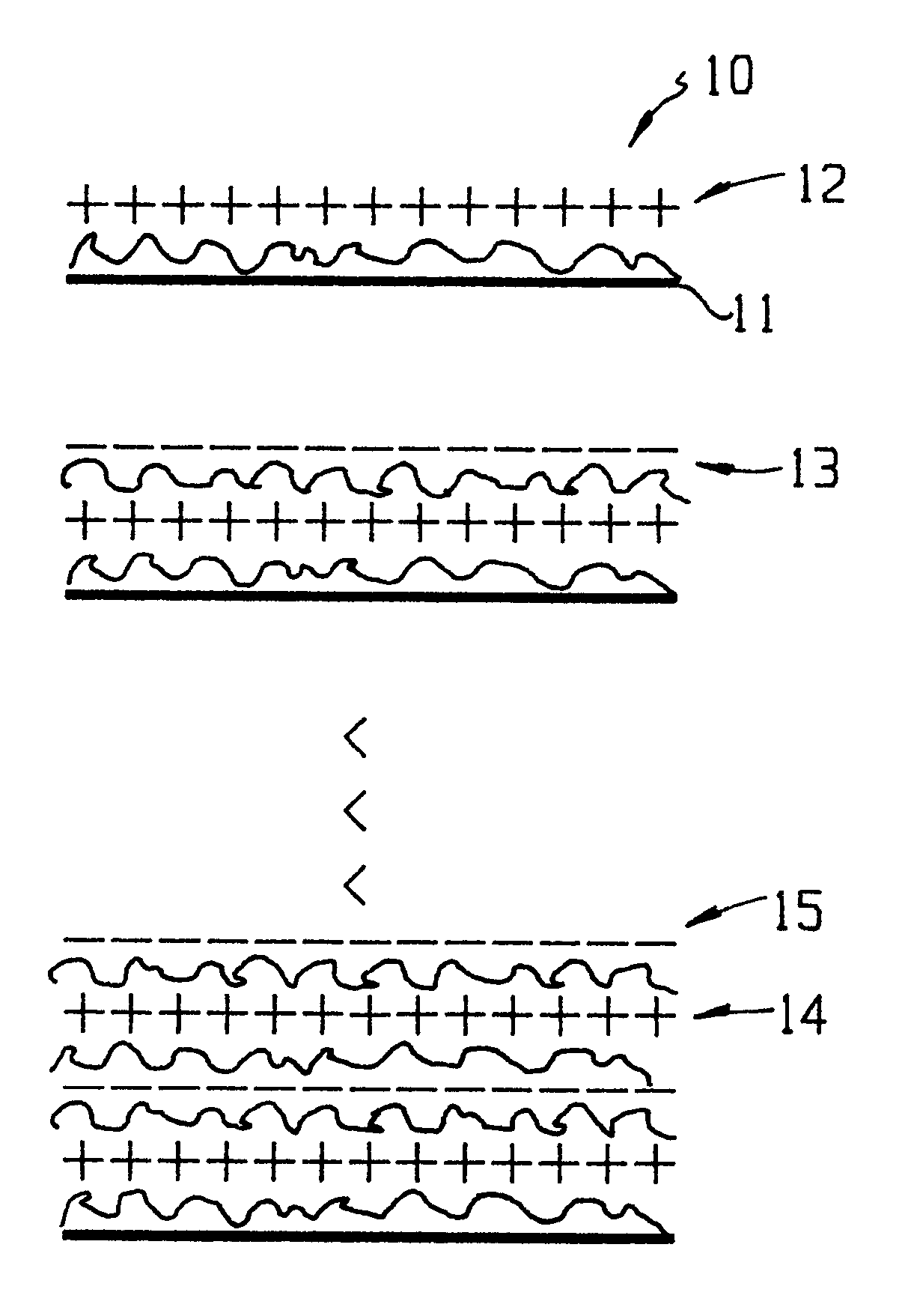
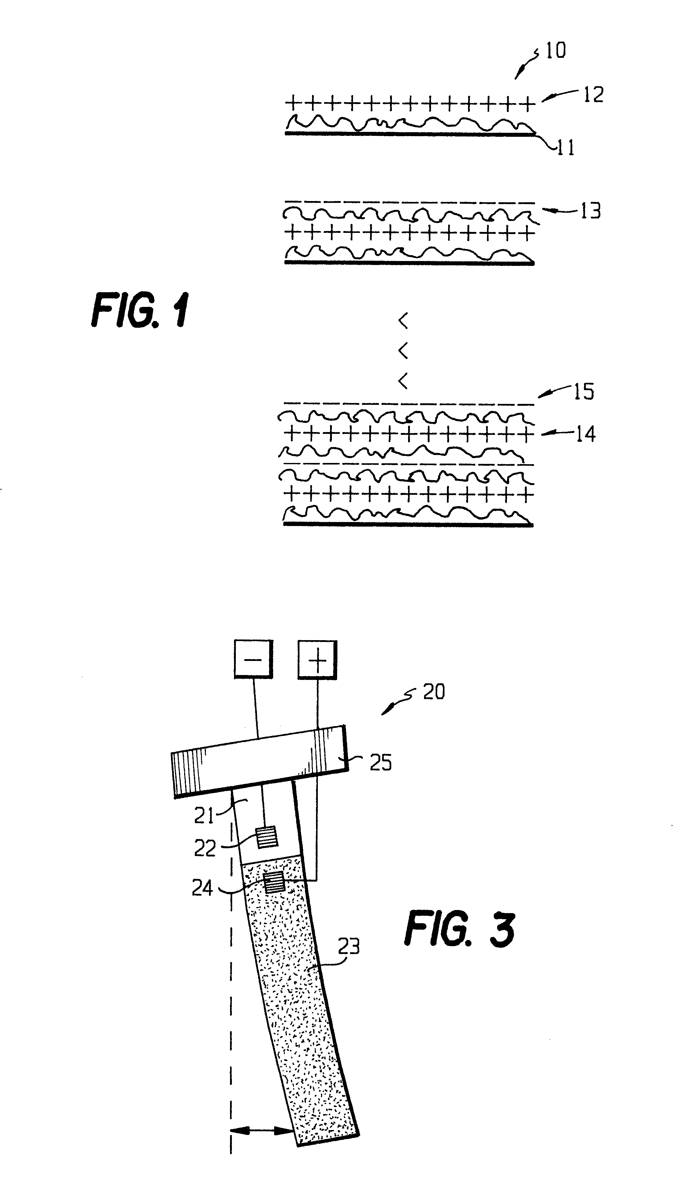
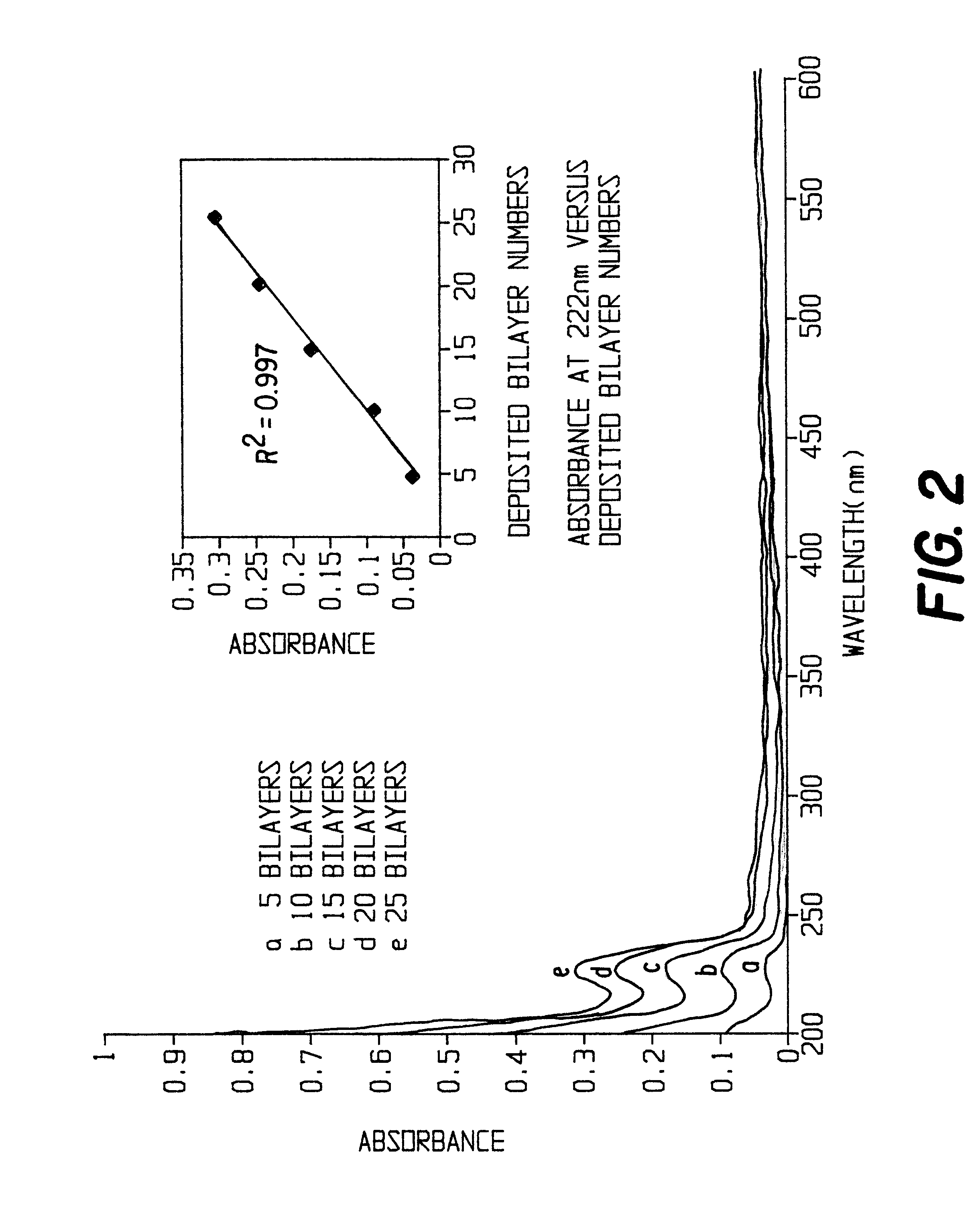
An electrostrictive and piezoelectric thin film assembly comprising poly(sodium 4-styrenesulfonate) ("PSS") and poly(diallyldimethylammonium chloride)("PDDA") was prepared by the ESA process. PSS was employed because its charged --SO.sub.3.sup.- functional group effectively gives it a noncentrosymmetric dipolar structure. PDDA was used as the counter ion to self-assemble the PSS. Both PSS (M.sub.w =70,000) and PDDA (M.sub.w =.about.400,000.about.500,000, 20 wt % in water) are commercially available from Aldrich Chemical Co.

The fabrication of the PSS / PDDA monolayer and multilayer films was carried out as follows. The substrates used were single-crystal p-111 silicon, quartz, and indium tin oxide ("ITO")-coated glass. Silicon and quartz substrates were pretreated with a 30:70 mixture of 30% hydrogen peroxide (H.sub.2 O.sub.2) and concentrated sulfuric acid (H.sub.2 SO.sub.4) for 30 minutes at room temperature, then rinsed extensively with Milli-Q water under ultrasonic agitation. The ...


PUM

PropertyMeasurementUnit
thicknessaaaaaaaaaa
thicknessaaaaaaaaaa
thicknessaaaaaaaaaa

Abstract

An electrostatic self-assembly method of fabricating electrostrictive and piezoelectric thin film assemblies not only provides a thinner film than is attainable by conventional methods, but provides excellent molecular-level uniformity and precise structural control, and thus large, effective piezoelectric coefficients. The method produces a thin film assembly including (a) a substrate, and (b) a film having one or a plurality of layers disposed upon the substrate, wherein at least one of the layers includes a dipolar material, and this layer of dipolar material has a uniform thickness of at most 500 nm.

Description

1. Field of the InventionThis invention relates generally to a thin film assembly, and a method of fabricating such a thin film assembly, which exhibits electrostrictive and / or piezoelectric properties. The invention relates more specifically to a method of fabricating electrostrictive and piezoelectric thin film assemblies which provides excellent molecular-level uniformity and precise structural control.2. Description of Related ArtElectrostrictive and piezoelectric materials have attracted great attention recently for use in sensors, microelectromechanical system ("MEMS") devices, and actuators. Electrostrictive materials produce displacement in reaction to an applied electric field. That is, when an electric field is applied, molecular-level polarization may change the dimensions of the material.Piezoelectric materials, conversely, produce an electrical charge displacement when mechanically strained. This charge displacement is associated with an electric field applied over a sp...

Claims


Application Information

Patent Timeline
Patent Type & Authority Patents(United States)
IPC IPC(8): H01L41/26H01L41/22
CPCH01L41/37H01L41/183B82Y30/00Y10T428/1259Y10T428/24917Y10T428/26Y10T428/12535Y10T428/12556H10N30/852H10N30/857H10N30/077H10N30/092
Inventor CLAUS, RICHARD O.ZENG, TINGYINGLIU, YANJING
Owner VIRGINIA TECH INTPROP INC
Why Eureka
Try Eureka