Method of producing high-quality silicon single crystals

a single crystal, high-quality technology, applied in the direction of crystal growth process, polycrystalline material growth, under protective fluid, etc., can solve the problems of device characteristics deterioration, device defects, and device underperforman

Inactive Publication Date: 2002-10-01
SUMITOMO MITSUBISHI SILICON CORP
View PDF7 Cites 61 Cited by
  • Summary
  • Abstract
  • Description
  • Claims
  • Application Information

AI Technical Summary

Problems solved by technology

Therefore, there arises the problem of grown-in defects; micro-defects having latent origins in the process of single crystal growth manifest in such process of device production, possibly causing devices to underperform.
It is well known that dislocations in a silicon single crystal cause deterioration in characteristics of a device formed therefrom.
OSF deteriorate electric characteristics, for example increase the leakage current and these defects exist at a high density in the ring QSF.
The laser scattering tomography defects occurring as major defects in faster grown single crystals, however, have been shown to markedly deteriorate the dielectric strength of the gate oxide films, which are now fairly thin.
With the increase in device pattern fineness, in particular, the influence of such defects becomes significant, rendering it difficult to cope with the task of increasing the scale of integration.
However, such software can indeed estimate the temperature distribution under given conditions but cannot provide concrete controlling conditions for realizing a specific temperature distribution state in the single crystal surroundings.
However, the whole wafer surface does not always consist of a denuded region but grown-in defects are found on the periphery or in the central region in many instances.
It was judged, however, that the rotational speed of the single crystal cannot be varied widely from the generally employed range of rotational speed from the viewpoint of uniform dopant and other impurity distribution and of changes in shape of single crystals during pulling.
However, when single crystal pulling was carried out selecting the rotational speed of the crucible and of the single crystal in the above manner so that the whole wafer surface might be occupied by the denuded region, the diameter stability of the single crystal was apt to be disturbed halfway past the body length required of the single crystal and then it became impossible to obtain the denuded state to a satisfactory extent; thus, it was fairly difficult to grow the single crystal in a stable shape and in a denuded state over the whole length thereof.
However, the denuded region was somewhat inferior in stability.
In this case, even when the disappearance thereof due to diffusion to the surface or coalescence proceeds to a certain extent, these leave their traces within the crystal, causing manifestation of laser scattering tomography defects.

Method used


Image

  • Method of producing high-quality silicon single crystals
  • Method of producing high-quality silicon single crystals
  • Method of producing high-quality silicon single crystals

Examples


examples

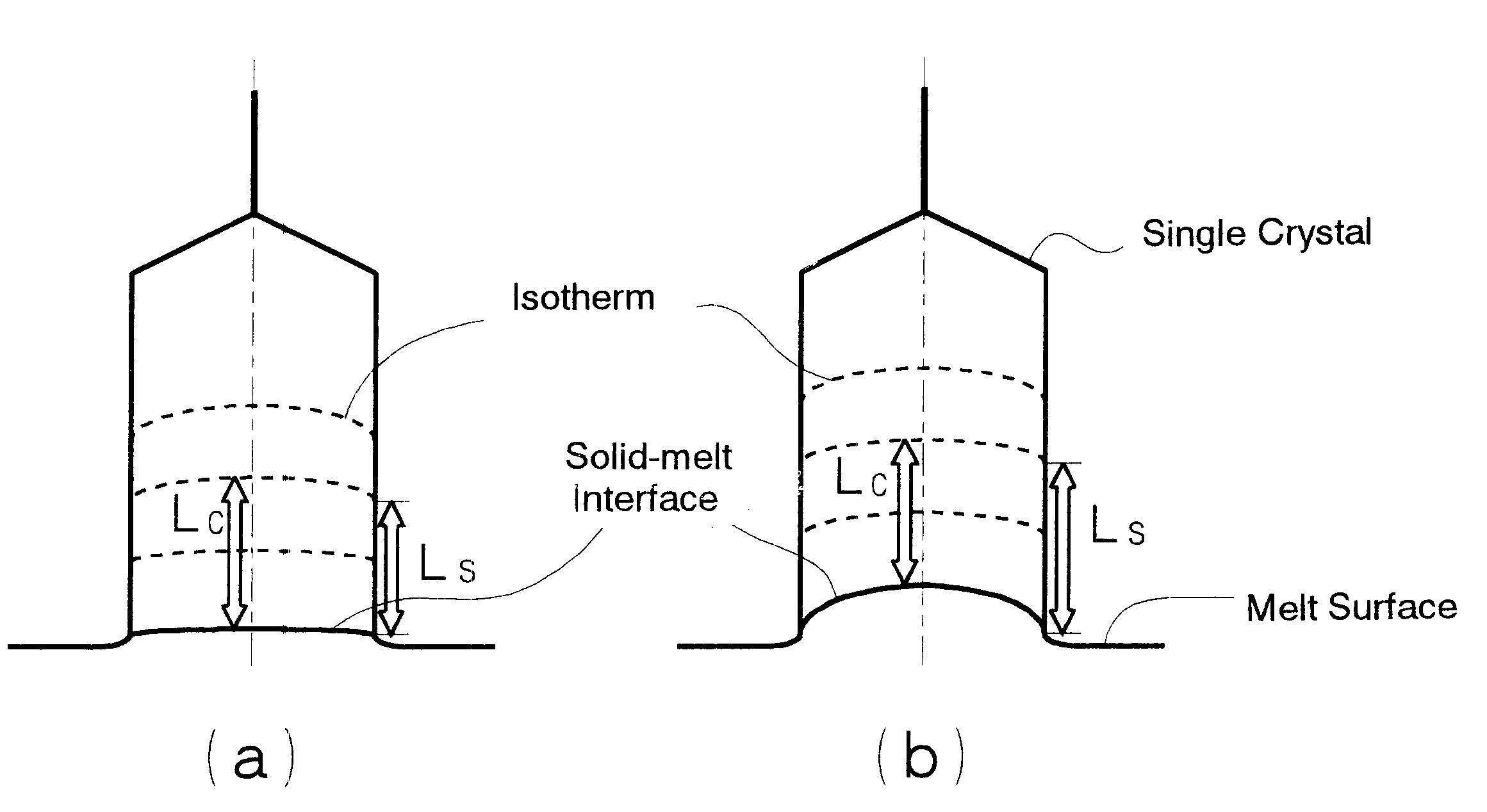
Using a single crystal puller allowing application of a horizontal magnetic field or cusped magnetic field, as shown in FIG. 5, 8-inch silicon single crystals were grown. Thus, a crucible la was charged with 120 kg of polycrystalline silicon as the starting material, and the p-type dopant boron was added thereto in an amount to give a crystal electric resistance of about 10 .OMEGA.cm. An argon atmosphere at 1,333 Pa was used as the atmosphere within the apparatus. The heat shield 7 used had a structure such that a cylindrical carbon felt body 7a with an inside diameter of 300 mm and a thickness of 50 mm was covered with a 7 mm-thick high purity graphite layer 7b. The shield was disposed so that the lower end thereof was 90 mm above the surface of the melt 3. An exciting coil 9 was disposed outside the stainless steel chamber 8 and a horizontal magnetic field or cusped magnetic field was applied by exchanging the coil.

The materials charged into the crucible la were heated by means of...


PUM

PropertyMeasurementUnit
magnetic fieldaaaaaaaaaa
melting pointaaaaaaaaaa

Abstract

A method of producing high-quality and large-diameter single crystals by the Czochralski method is disclosed which can provide wafers with a minimized number of such grown-in defects as dislocation clusters and laser scattering tomography defects. Specifically, it is a method of producing silicon single crystals which comprises carrying out the crystal pulling while maintaining the solid-melt interface during pulling in the shape of an upward convex with the central portion of the interface being higher by at least 5 mm than the peripheral region thereof and while applying a magnetic field, and optionally in addition to the above, while maintaining the temperature gradient in the direction of axis of pulling in the peripheral region at a level lower than that in the central portion in the range of from the melting point to 1,200° C. In this case, it is desirable that the portion of the single crystal surface lying at least 50 mm above the melt surface be shielded from direct radiant heat from the heater and / or crucible wall, that a horizontal magnetic field of 0.08 to 0.3 T be applied in parallel with the melt surface or a cusped magnetic field showing an intensity of 0.02 to 0.07 T at a crucible wall site on the melt surface be applied and that the crucible be rotated at a speed of not more than 5 min-1 and the single crystal at a speed of not less than 13 min-1.

Description

This invention relates to a method of producing silicon single crystals for use as semiconductor materials, namely silicon wafers. More particularly, it relates to a method of producing high-quality silicon single crystals for use as wafers, which are grown by the Czochralski method and free of grown-in defects.DESCRIPTION OF THE PRIOR ARTIt is Czochralski's method of growing single crystals that is most widely employed in the production of silicon single crystals for use as semiconductor silicon wafers.The Czochralski method comprises dipping a silicon seed crystal in molten silicon in a quartz crucible and then pulling up the seed from the melt while allowing single crystal growth. Advances in this silicon single crystal growing technology have made it possible to produce dislocation-free large single crystals with few defects. Semiconductor devices are produced by hundreds of process steps starting with wafers which are obtained from such single crystals and serve as substrates. ...

Claims


Application Information

Patent Timeline
Patent Type & Authority Patents(United States)
IPC IPC(8): C30B15/30C30B15/00C30B29/06C30B15/14C30B15/20H01L21/208
CPCC30B15/203C30B15/305C30B29/06C30B15/00C30B15/14
Inventor OKUI, MASAHIKOMURAKAMI, HIROKIEGASHIRA, KAZUYUKIITO, MAKOTOHAYAKAWA, HIROSHIGARRET, KELLYSHIRAKAWA, YOSHINORI
Owner SUMITOMO MITSUBISHI SILICON CORP
Why Eureka
Try Eureka