Silicon wafer including both bulk and SOI regions and method for forming same on a bulk silicon wafer

a technology of silicon wafers and bulk silicon, applied in the direction of semiconductor devices, electrical equipment, transistors, etc., can solve the problems of junction capacitance, increase power consumption, slow the speed at which devices using such transistors can operate, etc., to achieve faster operating speed, lower capacitance, and the effect of large current flow

Inactive Publication Date: 2002-10-15
GLOBALFOUNDRIES INC
View PDF37 Cites 66 Cited by
  • Summary
  • Abstract
  • Description
  • Claims
  • Application Information

AI Technical Summary

Benefits of technology

The SOI circuit portion may include SOI FETs and the bulk circuit portion may include bulk FETs, the SOI FETs having a lower capacitance and faster operating speed than the bulk FETs. Additionally, the bulk FETs may have a larger current flow and generate more heat than the SOI FETs. The bulk circuit portion may include input/output buffer circuits and electrostatic damage (ESD) protection circuits. The ESD protection circuits may couple a plurality of controlled collapse chip connection terminals (C4 terminals) to the input/output buffer circuits. The C4 terminals may couple and bond the circuit to an IC package or a printed circuit board. A second aspect of the pres

Problems solved by technology

This is undesirable for the current industry goals for size reduction.
Additionally, junction capacitance between the source/drain and the bulk substrate and "off" state leakage from the drain to the source both increase power consumption.
Junction capacitance also slows the speed at which a device using such transistors can operate.
These problems result in difficulties in reducing the size, power consumption, and voltage of CMOS technology devices.
One problem with forming field effect transistors on an SOI wafer is the floating body effect.
The floating body effect causes the current-to-voltage curve for the transistor to distort or kink, which in turn causes the threshold voltage for operating the transistor to fluctuate.
This problem is p

Method used


Image

  • Silicon wafer including both bulk and SOI regions and method for forming same on a bulk silicon wafer
  • Silicon wafer including both bulk and SOI regions and method for forming same on a bulk silicon wafer
  • Silicon wafer including both bulk and SOI regions and method for forming same on a bulk silicon wafer

Examples


Embodiment Construction

The present invention will now be described in detail with reference to the drawings. In the drawings, like reference numerals are used to refer to like elements throughout.

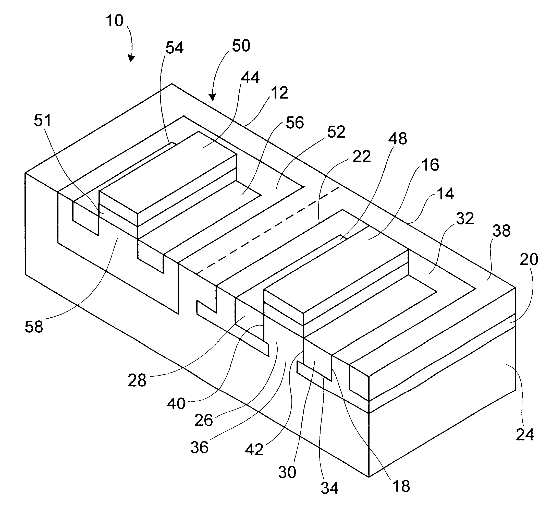
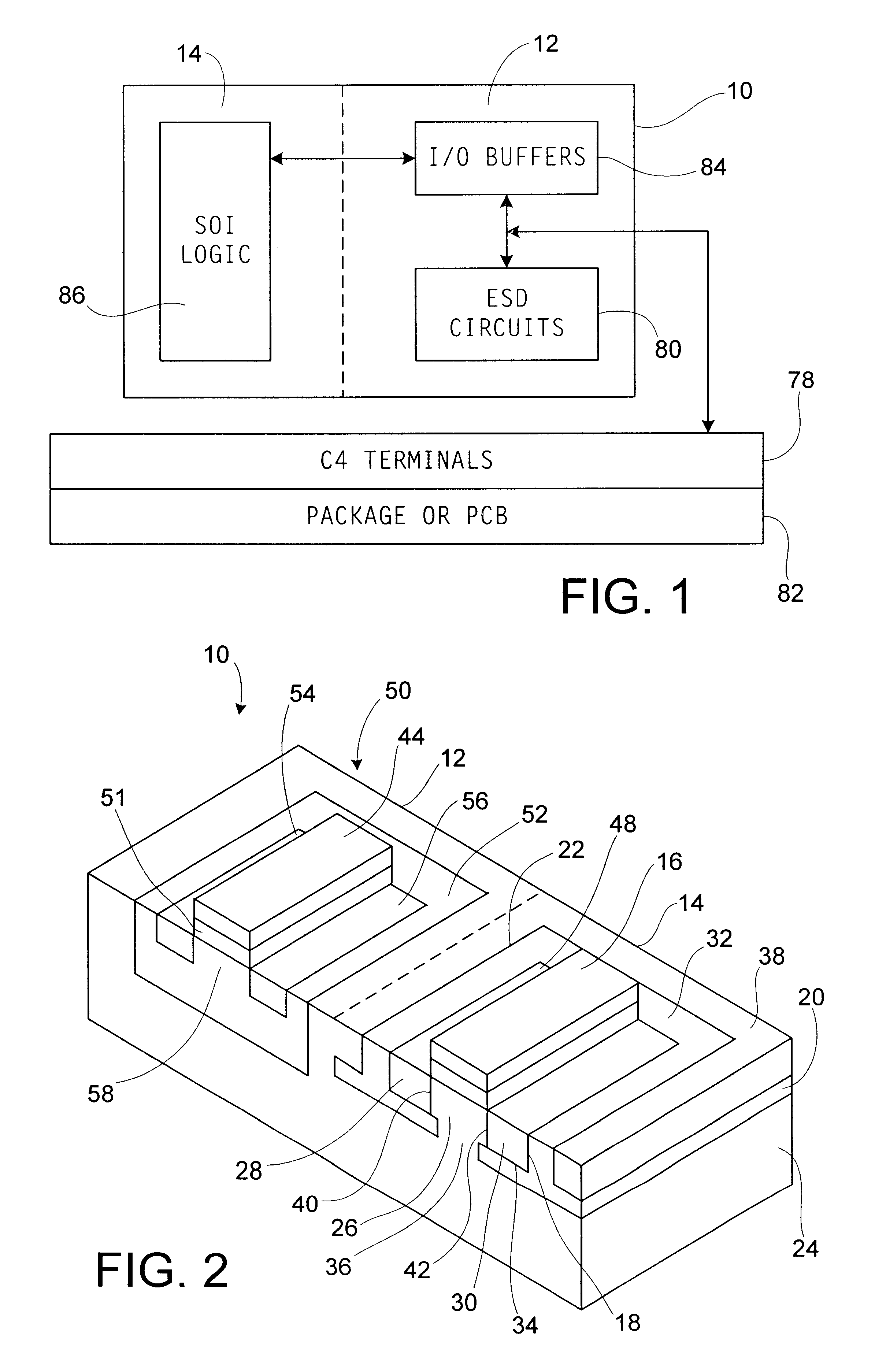
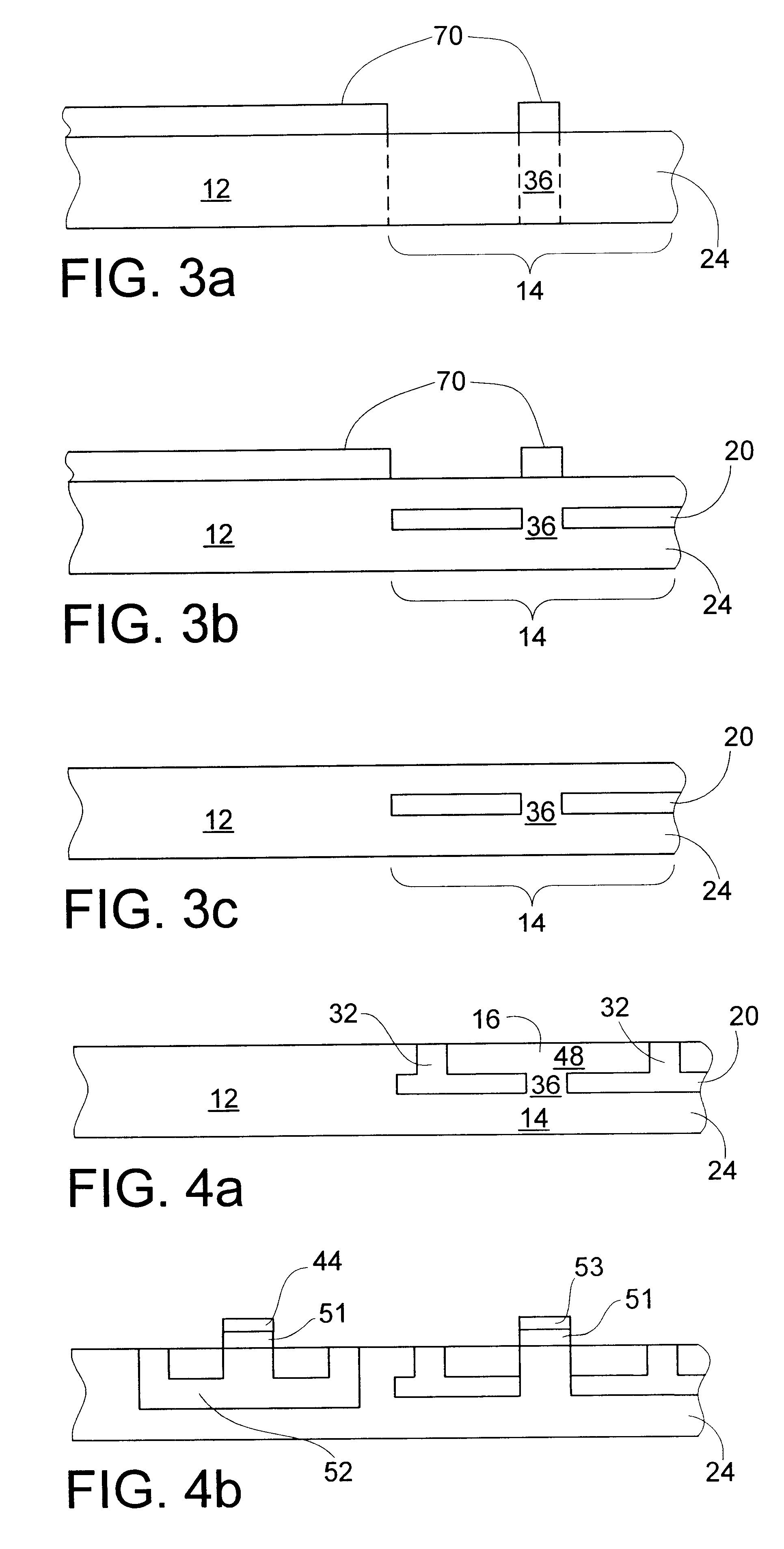
Referring to FIG. 1, circuit 10 includes a bulk region 12 and a silicon-on-insulator (SOI) region 14. SOI region 14 includes SOI logic circuits 86 including a plurality of SOI field effect transistors (FETs). As discussed previously, SOI FETs have low capacitance and can operate at faster clock speeds making the SOI logic circuits advantageous for implementing high speed logic. Bulk region 12 includes bulk circuits such as input / output (I / O) buffer circuits 84 and electrostatic damage (ESD) protection circuits 80. Bulk field effect transistors can typically handle larger current flows without damage and can more quickly dissipate heat than SOI FETs. Therefore, bulk region 12 is advantageous for implementation of I / O buffer circuits 84 and ESD protection circuits 80.

The SOI logic circuits 86 are coupled to the I / O...


PUM


Abstract

A silicon substrate comprises a silicon-on-insulator (SOI) portion which includes an insulating silicon dioxide layer beneath a device layer. SOI circuit structures, including SOI field effect transistors, are formed in the device layer. The substrate also comprises a bulk portion. Bulk semiconductor circuit structures are formed in wells in the bulk portion. The bulk circuit structures may be coupled to the SOI circuit structures.

Description

TECHNICAL FIELDThe present invention relates generally to silicon-on-insulator (SOI) structures, and more specifically to SOI substrate structures advantageous in the fabrication of SOI transistors and bulk structures on the same substrate.BACKGROUND OF THE INVENTIONConventional or bulk semiconductor devices are formed in semiconductive material by implanting a well of either P-type or N-type conductivity silicon in a silicon substrate wafer of the opposite conductivity. Gates and source / drain diffusions are then manufactured using commonly known processes. These form devices known as metal-oxide-semiconductor (MOS) field effect transistors (FETs). When a given chip uses both P-type and N-type, it is known as a complimentary metal oxide semiconductor (CMOS). Each of these transistors must be electrically isolated from the others in order to avoid shorting the circuits. A relatively large amount of surface area is needed for the electrical isolation of the various transistors. This i...

Claims


Application Information

Patent Timeline
IPC IPC(8): H01L21/336H01L21/70H01L21/762H01L29/02H01L29/06H01L21/02H01L29/786H01L21/8234H01L29/66H01L21/266H01L21/265
CPCH01L21/76264H01L21/823418H01L21/823481H01L29/0653H01L29/66636H01L29/78609H01L21/26533H01L21/266Y10S257/901
Inventor JU, DONG-HYUK
Owner GLOBALFOUNDRIES INC
Why Eureka
Try Eureka