

Multilayer printed wiring board having a roughened inner conductor layer and production method thereof
a printing method and wiring board technology, applied in the direction of dielectric characteristics, insulating substrate metal adhesion improvement, circuit masks, etc., can solve the problems of preventing the obstruction of the curing reaction through oxygen, causing cracks, and affecting the appearance of the wiring board, so as to prevent the obstruction of the curing reaction. , the effect of poor mounting
- Summary
- Abstract
- Description
- Claims
- Application Information
AI Technical Summary
Benefits of technology
Problems solved by technology
Method used
Image

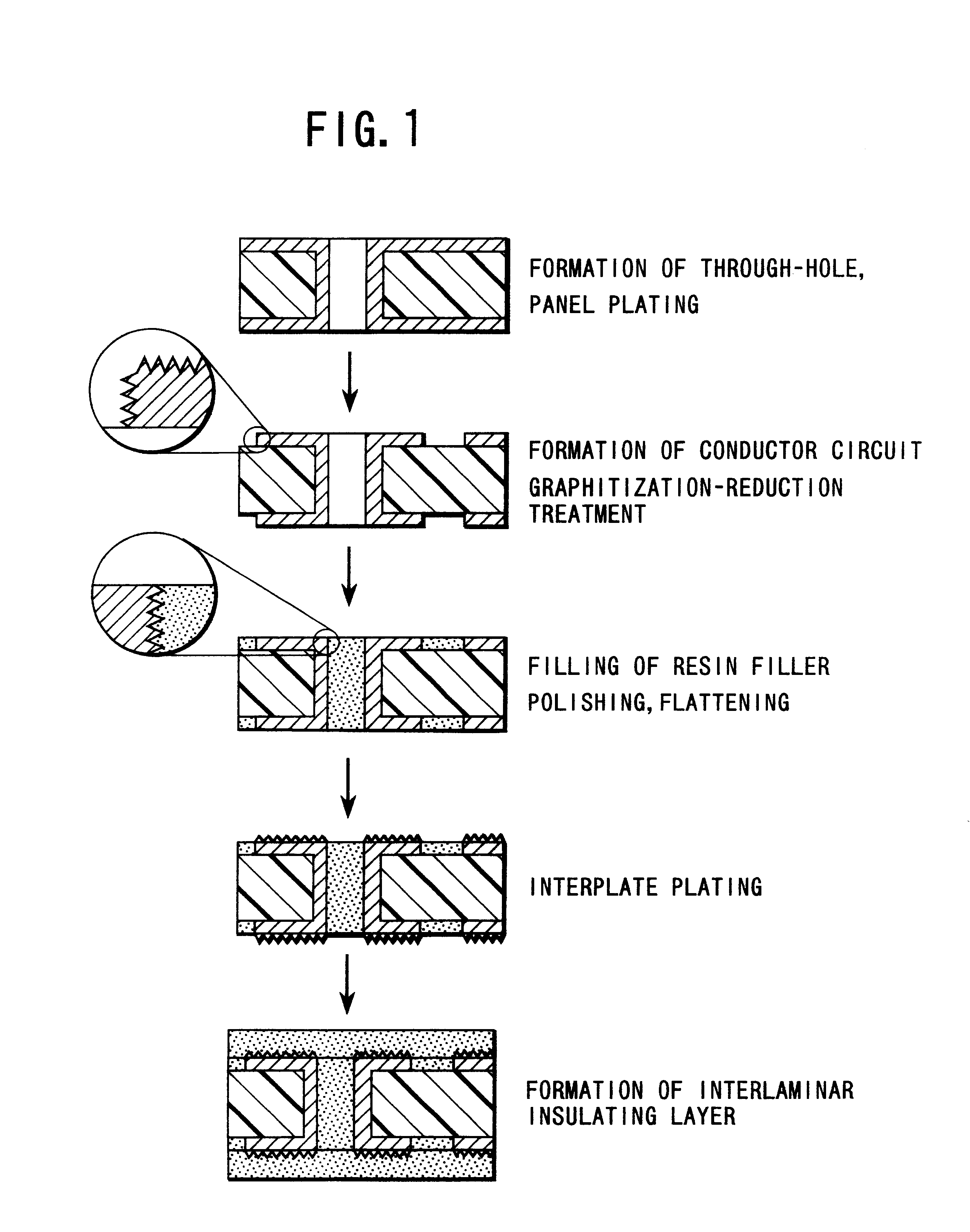
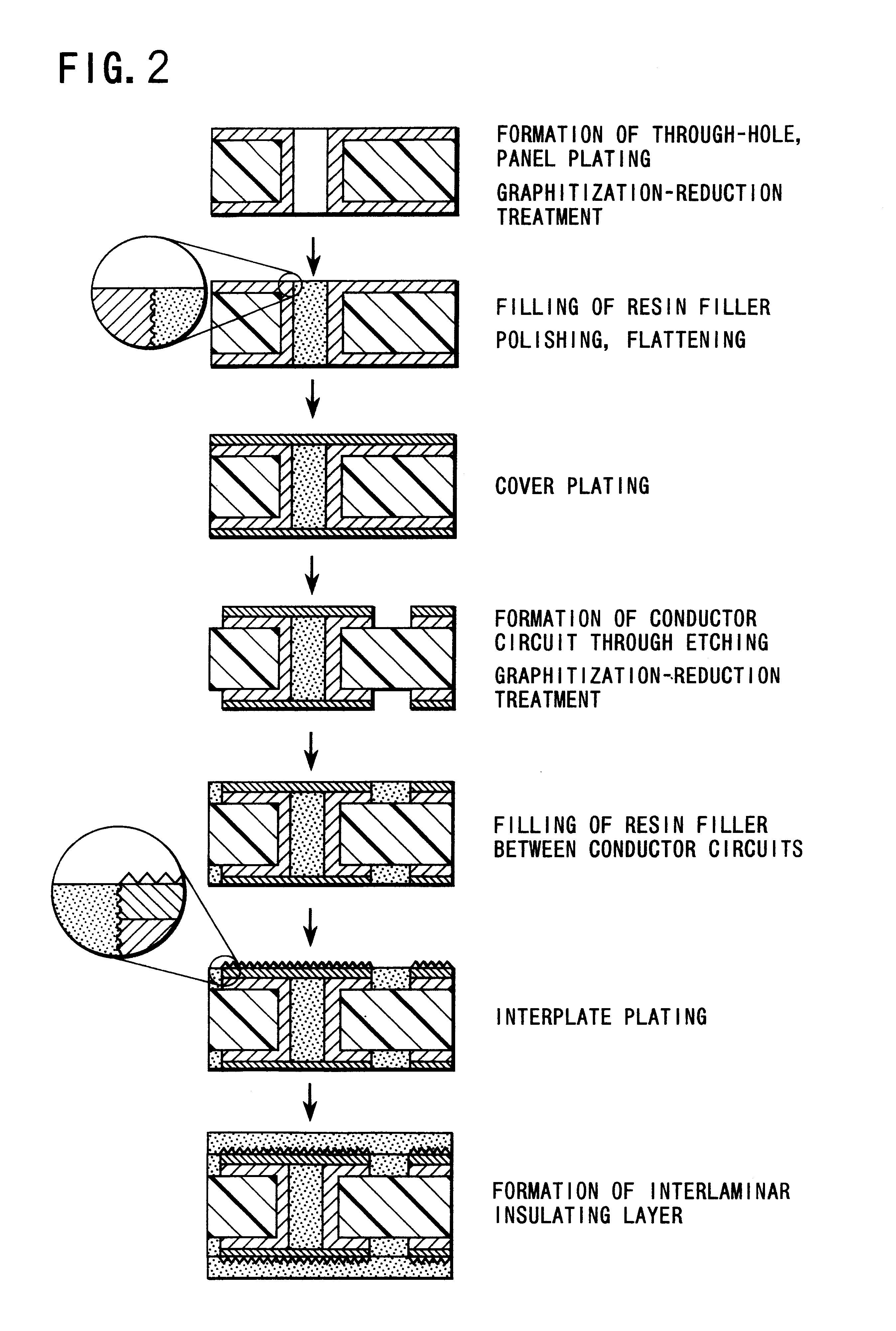
Examples
example 2
(1).about.(3) The treatment is carried out according to the same steps as in the items (1).about.(3) of Example 1.
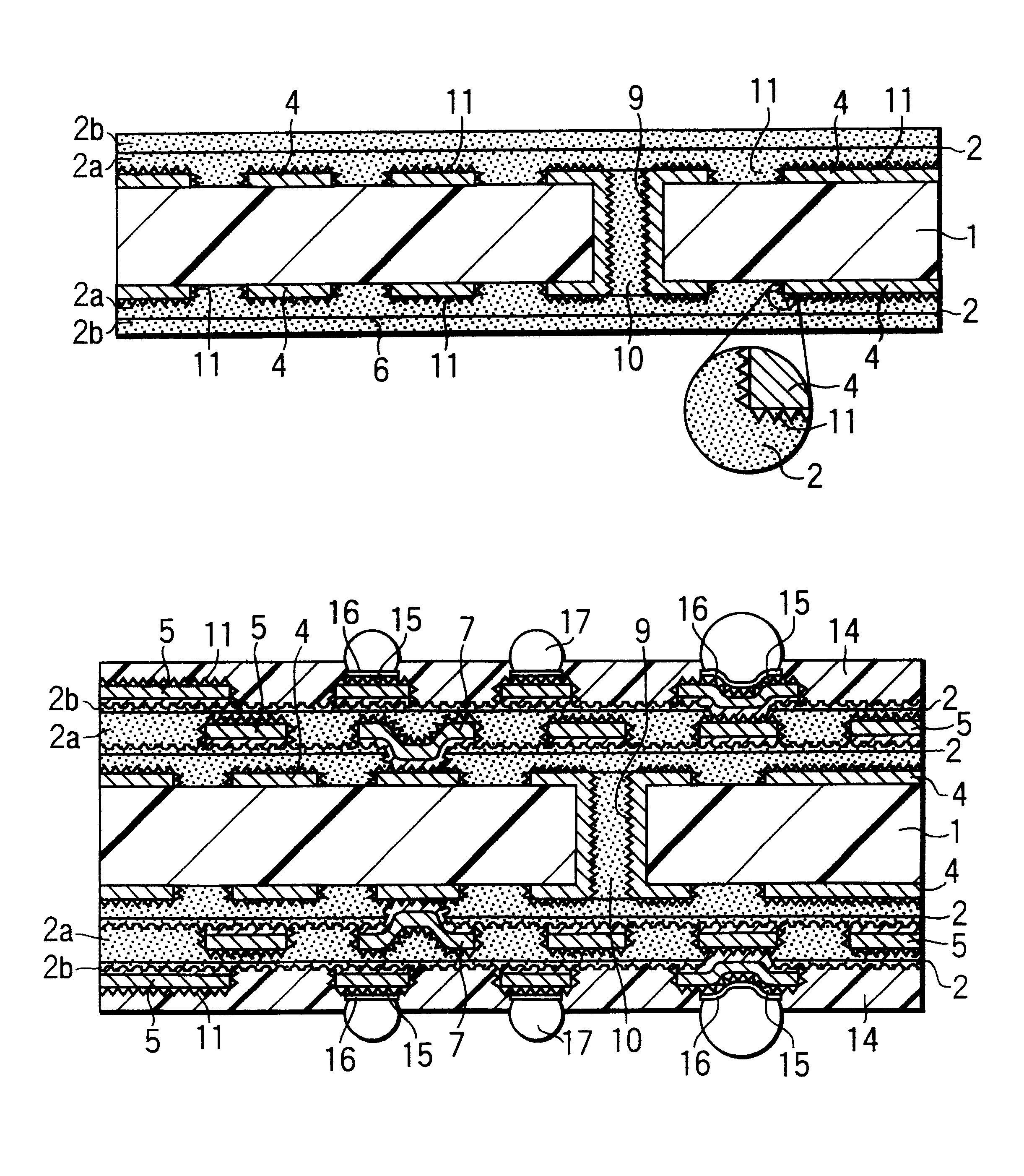
(4) Then, the copper foil is treated according to usual manner, for example, by etching with an aqueous solution of ferric chloride or the like to form inner conductor circuit patterns and through-hole land (see FIG. 8).
To the full surface including side faces of the inner conductor circuit patterns 5 and the through-hole lands is sprayed an etching solution comprising 10 parts by weight of imidazole copper (II) complex, 7 parts by weight of glycolic acid and 5 parts by weight of potassium chloride, i.e. "Mechetchbond", trade name of Mech Corporation, which is transferred to conduct the etching, whereby a roughened layer is formed. The resulting roughened surface has a height of 3 .mu.m. (Tin layer is not formed.) (5).about.(12) The treatment is carried out according to the same steps as in the items (5).about.(12) of Example 1.
(13) The substrate provided with the inner ...
example 3
A. Preparation of Adhesive for Electroless Plating as Upper Layer
1. 35 parts by weight of a resin solution of 25% acrylate of cresol novolac type epoxy resin (made by Nippon Kayaku Co., Ltd., molecular weight: 2500) dissolved at a concentration of 80 wt % in DMDG is mixed with 3.15 parts by weight of a photosensitive monomer (made by Toa Gosei Co., Ltd., Aronix M315), 0.5 part by weight of an anti-foaming agent (made by Sannopuco, S-65) and 3.6 parts by weight of NMP with stirring.
2. 12 parts by weight of polyether sulphone (PES) is mixed with 7.2 parts by weight of epoxy resin particles (made by Sanyo Kasei Co., Ltd., Polymerpol) having an average particle size of 1.0 .mu.m and 3.09 parts by weight of the resin particles having an average particle size of 0.5 .mu.m, and further added with 30 parts by weight of NMP, which are mixed in a bead mill with stirring.
3. 2 parts by weight of an imidazole curing agent (made by Shikoku Kasei Co., Ltd., 2E4MZ-CN) is mixed with 2 parts by weigh...
example 4
(1) The treatment is carried out according to the same steps as in the items (1).about.(7) of Example 3.
(2) To the full surface including side faces of the inner conductor circuit patterns 29 and side faces of the conductor layer 30 covering the filler 25 is sprayed an etching solution comprising 10 parts by weight of imidazole copper (II) complex, 7 parts by weight of glycolic acid and 5 parts by weight of potassium chloride, i.e. "Mechetchbond", trade name of Mech Corporation, which is transferred to conduct the etching, whereby a roughened layer is formed. The resulting roughened surface has a height of 3 .mu.m. (Tin layer is not formed.)
(3) The treatment is carried out according to the same steps as in the items (9).about.(16) of Example 3.
(4) To the full surface including side faces of the outer conductor circuit patterns 29 and side face of the conductor layer 30 covering the filler 25 is sprayed an etching solution comprising 10 parts by weight of imidazole copper (II) comple...
PUM
| Property | Measurement | Unit |
|---|---|---|
| Temperature | aaaaa | aaaaa |
| Electrical resistance | aaaaa | aaaaa |
| Transparency | aaaaa | aaaaa |
Abstract
Description
Claims
Application Information