Method of forming vias in silicon carbide and resulting devices and circuits

a silicon carbide and via technology, applied in semiconductor devices, semiconductor device details, electrical apparatus, etc., can solve the problems of limiting the gain that can be delivered at high frequencies, affecting the performance and affecting the efficiency of silicon carbide devices

Inactive Publication Date: 2003-02-04
WOLFSPEED INC
View PDF29 Cites 148 Cited by
  • Summary
  • Abstract
  • Description
  • Claims
  • Application Information

AI Technical Summary

Benefits of technology

Therefore, it is an object of the present invention to provide a method of etching vias in and entirely through silicon car

Problems solved by technology

For example, although discrete (i.e., individual) silicon (Si) based devices can operate at microwave frequencies, silicon-based integrated circuits suffer from lower electron mobility and are generally disfavored for frequencies above about 3-4 Ghz.
Silicon's inherent conductivity also limits the gain that can be delivered at high frequencies.
Although wire bonding techniques can be used for other devices that operate at other frequencies, they are disadvantageous at microwave frequencies in silicon carbide devices.
In particular, wires tend to cause undesired inductance at the microwave frequencies at which silicon carbide devices are capable of operating.
To date, however, opening vias in silicon carbide has been rather difficult because of its extremely robust physical characteristics, which, as noted above, are generally advantageous for most other purposes.
Silicon carbide does not lend itself rapidly to wet etching because of SiC's stability and high

Method used


Image

  • Method of forming vias in silicon carbide and resulting devices and circuits
  • Method of forming vias in silicon carbide and resulting devices and circuits
  • Method of forming vias in silicon carbide and resulting devices and circuits

Examples


Embodiment Construction

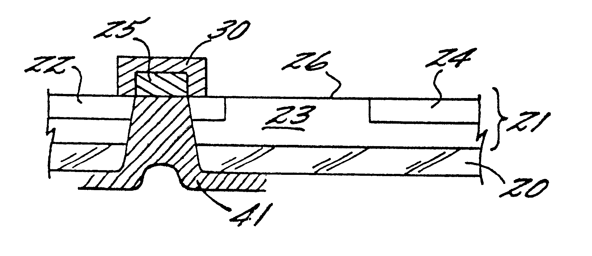
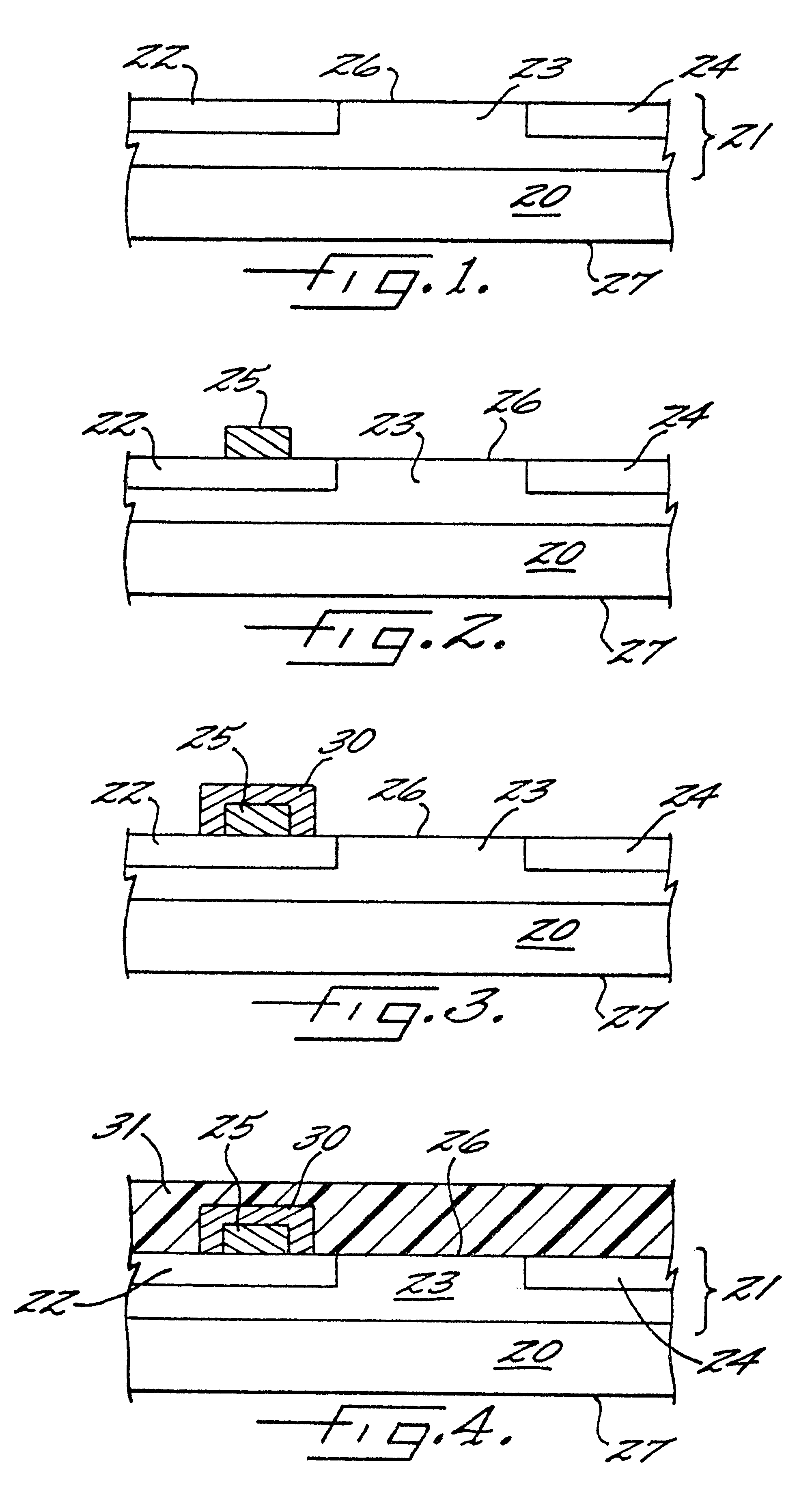
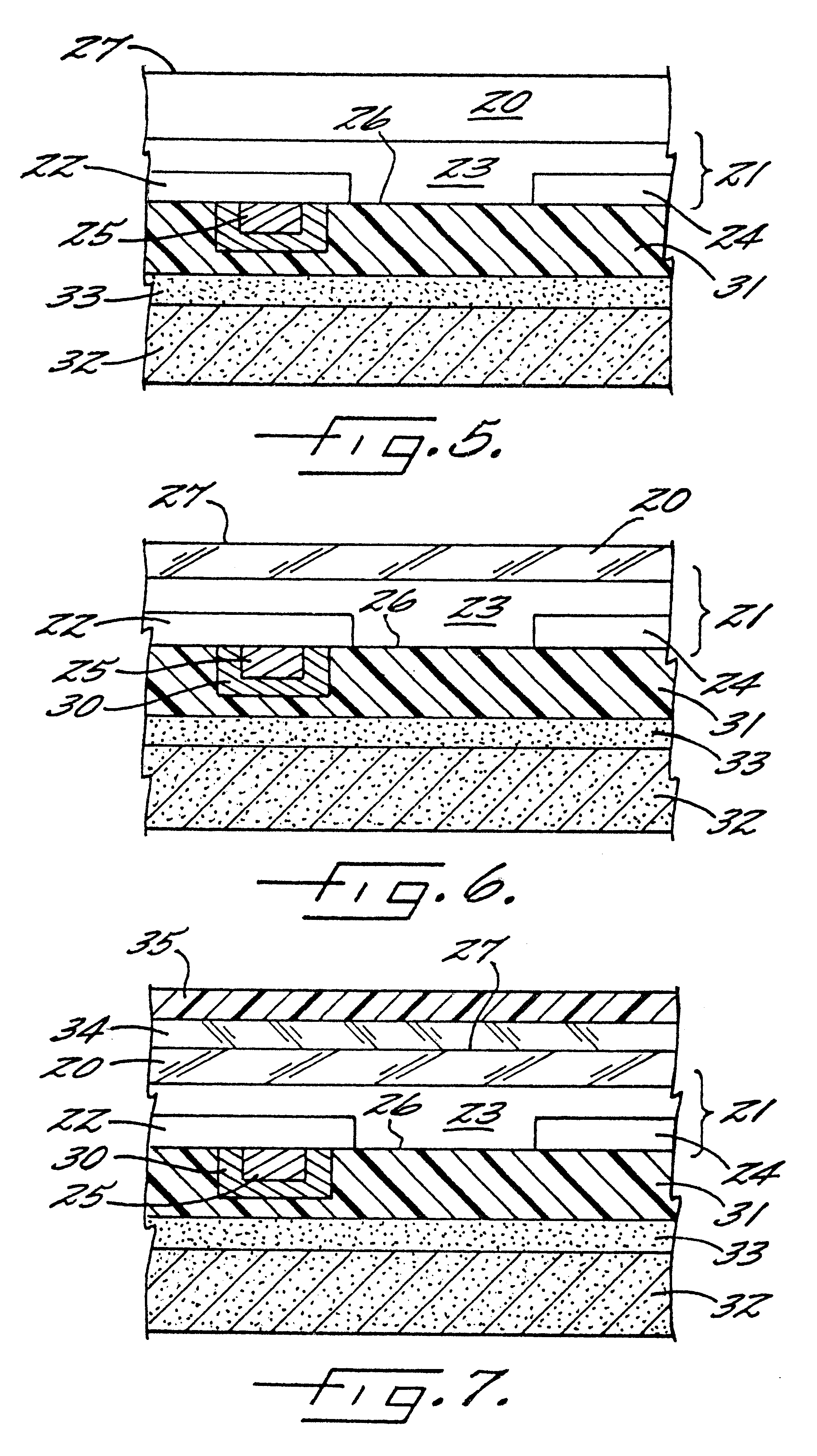
In preferred embodiments, the present invention also comprises a method of dry etching a via in SiC using sulfur hexafluoride chemistry in an inductively coupled plasma (ICP). In a particular embodiment of the invention, the dry etching was conducted in a Model 790 ICP system manufactured by Plasma-Therm Incorporated.

In this system, the wafer is placed on a He-cooled chuck in the process chamber, the wafer is clamped and subsequently the process chamber is evacuated to 10.sup.-5 Torr with a turbo and mechanical pump. Five to twenty cubic centimeter per minute electronic grade sulfur hexafluoride is injected into the process chamber and a butterfly valve above the turbo pump is throttled to achieve the operating pressure of 2 to 5 mT. Subsequently, power is applied to generate a plasma. This system uses two radio frequency (RF) power sources. One is connected to the chuck and is used to control energies of ions reaching the substrate and is set between 1 to 2 W / cm.sup.2. The second R...


PUM


Abstract

A method of fabricating an integrated circuit on a silicon carbide substrate is disclosed that eliminates wire bonding that can otherwise cause undesired inductance. The method includes fabricating a semiconductor device on a first surface of a silicon carbide substrate and with at least one metal contact for the device on the first surface of the substrate. The opposite, second surface of the substrate is then ground and polished until it is substantially transparent. The method then includes masking the polished second surface of the silicon carbide substrate to define a predetermined location for a via that is opposite the device metal contact on the first surface; etching the desired via through the desired masked location until the etch reaches the metal contact on the first surface; and metallizing the via to provide an electrical contact from the second surface of the substrate to the metal contact and to the device on the first surface of the substrate.

Description

The present invention relates to integrated circuits formed in semiconductor materials and in particular relates to methods for forming via openings in semiconductor substrates and the resulting structures. More particularly, the invention relates to the use of such vias to form monolithic microwave integrated circuits (MMICs) in silicon carbide (SiC).The present invention relates to the manufacture of via openings ("vias") in integrated circuits (ICs), and in particular relates to a method of forming such vias in silicon carbide in order to take advantage of silicon carbide's electronic, thermal, and mechanical properties in the manufacture and use of monolithic microwave integrated circuits.MMICsIn its most basic sense, a monolithic microwave integrated circuit is an integrated circuit; i.e., a circuit formed up a plurality of devices; in which all of the circuit components are manufactured on top of a single semiconductor substrate, and which is designed to operate at microwave f...

Claims


Application Information

Patent Timeline
IPC IPC(8): H01L21/70H01L21/768H01L21/04H01L21/02H01L21/28H01L21/3205H01L23/52
CPCH01L21/0445H01L21/76898H01L2924/0002H01L2924/00H01L29/1608H01L21/28
Inventor RING, ZOLTAN
Owner WOLFSPEED INC
Why Eureka
Try Eureka