
Reticles including support frame for charged-particle-beam microlithography, and methods for making same

a technology of microlithography and support frame, which is applied in the direction of manufacturing tools, electric/magnetic/electromagnetic heating, instruments, etc., can solve the problems of inability to develop a practical x-ray system, the x-ray system has not yet been developed, and the resolution limitations of optical microlithography have become apparent. , to achieve the effect of reducing the stress generated in the reticle membrane 56, reducing distortion, and reducing the overall distortion of the reticle membran

Inactive Publication Date: 2003-03-18
NIKON CORP
View PDF6 Cites 18 Cited by
  • Summary
  • Abstract
  • Description
  • Claims
  • Application Information

AI Technical Summary

Benefits of technology

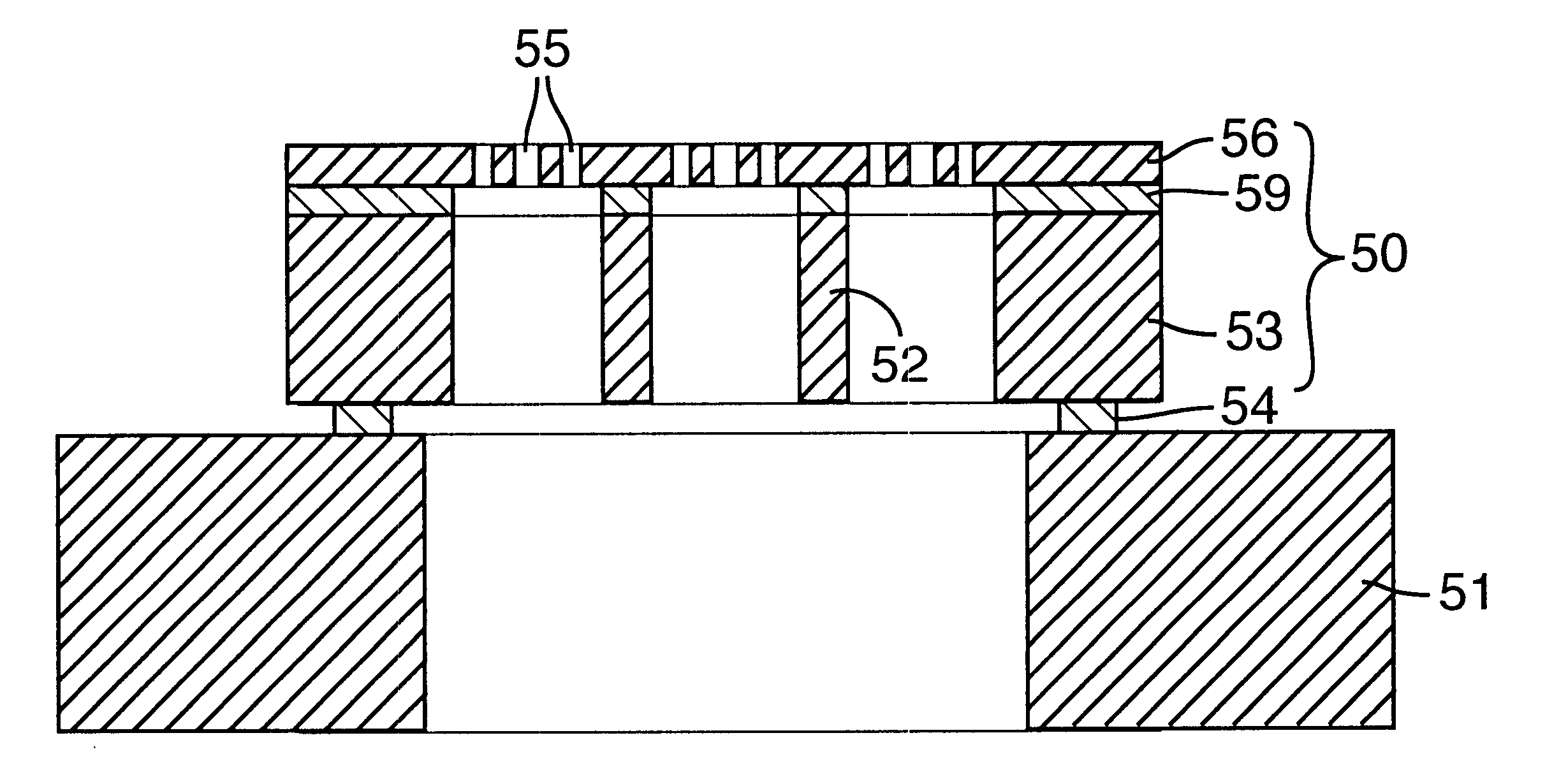
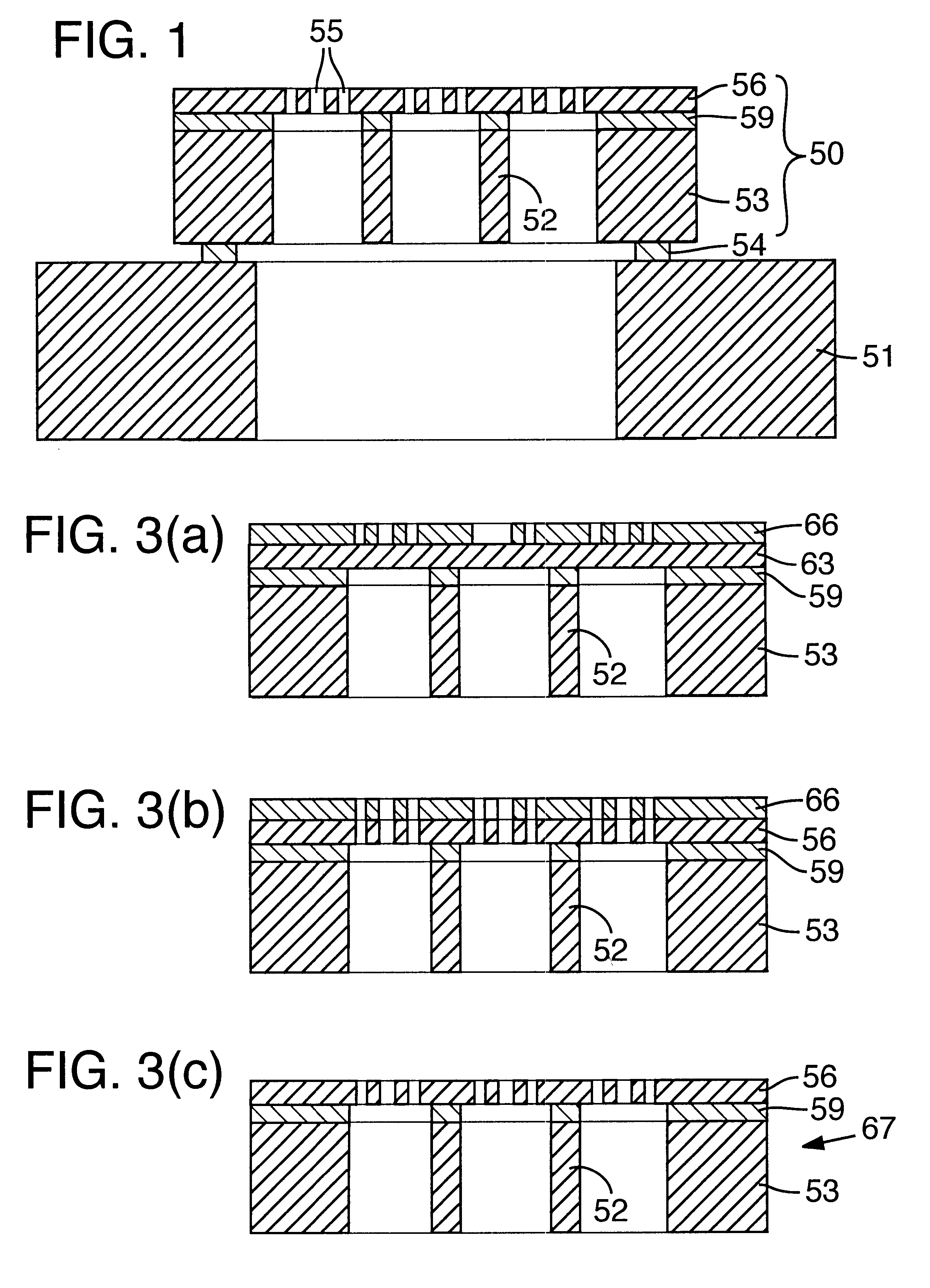
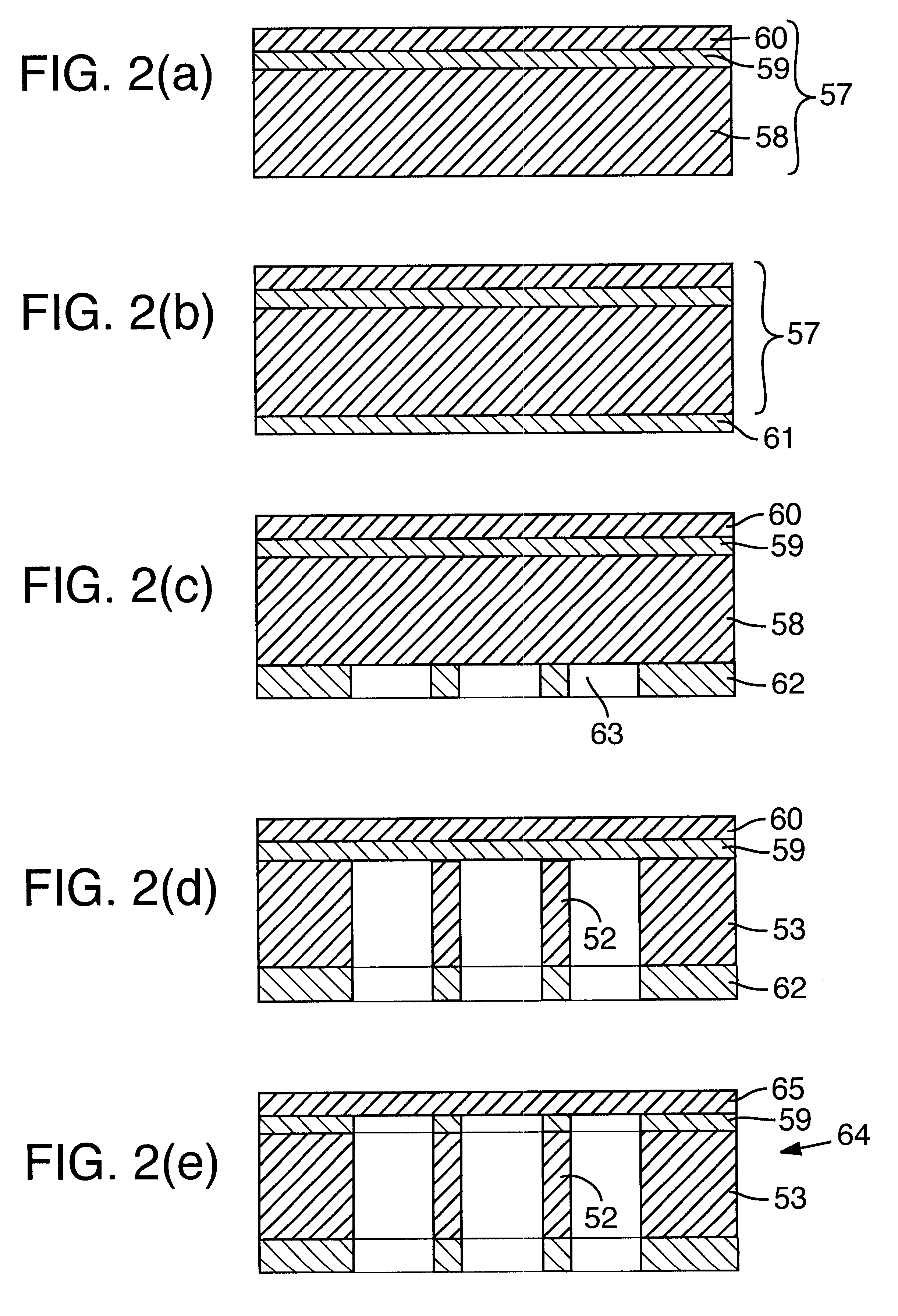
This embodiment is depicted in FIG. 1, showing a reticle 50 for charged-particle-beam (CPB) microlithography, bonded to a support frame 51. The reticle 50 comprises support struts 52 and a peripheral frame 53 made of silicon. The support frame 51 also is made of silicon. The support frame 51 is bonded by anodic welding to the peripheral frame 53 via a thin glass plate 54 containing mobile ions (e.g., sodium ions). The mobile ions facilitate formation of a space-charge region at the glass-silicon interface upon application of a dc voltage for performing anodic welding. The space-charge region, in turn, facilitates formation of a strong glass-silicon weld during anodic welding. By "thin" is meant that the glass has a thickness range of 1 to 50 micrometers.
In this representative embodiment, since the peripheral frame 53 and support frame 51 are bonded together via the intervening small regions 73 of glass (which are thin), the stress generated in the reticle membrane 56 is reduced markedly, which provides a correspondingly reduced distortion in the pattern defined in or on the reticle membrane 56. In addition, using small regions 73 of glass to effect bonding results in localization of distortion-generating areas, thereby further reducing overall distortion of the reticle.

Problems solved by technology

In recent years, as semiconductor integrated circuits increasingly have become miniaturized, the resolution limitations of optical microlithography (i.e., microlithography performed using ultraviolet light as an energy beam) increasingly have become apparent.
For example, considerable effort has been directed to use of X-rays.
However, a practical X-ray system has not yet been developed because of many technical problems with that technology.
However, with such systems, the more intricate the pattern, the more focused the electron beam must be in order to render the pattern satisfactorily.
Also, drawing a pattern line-by-line requires large amounts of time; consequently, this technology has very little utility in the mass production of semiconductor wafers where "throughput" (number of wafers processed per unit time) is an important consideration.
Unfortunately, under such conditions, distortion of the weld joint usually occurs, due to the stated differences in coefficients of thermal expansion, as the welds return to room temperature after completion of welding.
Having to attain such temperatures for bonding purposes is problematic because of the time required to reach bonding temperature.
Also, this technique requires robust and costly equipment.
An additional problem arises in the fact that the membrane surface of a finished reticle, as well as the reticle support, must be cleaned regularly using chlorine gas or the like to maintain cleanliness of the reticle.
Exposure of eutectically bonded surfaces to chlorine gas causes corrosion of the bonds.
As a result, weld-joint distortion develops from the differences in the coefficients of thermal expansion of silicon versus the bonding metal (e.g., aluminum).

Method used


Image

  • Reticles including support frame for charged-particle-beam microlithography, and methods for making same
  • Reticles including support frame for charged-particle-beam microlithography, and methods for making same
  • Reticles including support frame for charged-particle-beam microlithography, and methods for making same

Examples


example 2

An SOI substrate was prepared having a diameter of 8 inches. A reticle blank was fabricated according to the process shown in FIGS. 2(a)-2(e).

A silicon support frame was fabricated having an OD of 230 mm, an ID of 190 mm, and an axial thickness of 6 mm. A glass member (Corning 7740 Pyrex.TM.) was fabricated having an OD of 200 mm, an ID of 190 mm, and an axial thickness of 1 mm. The support frame and glass member were bonded together by anodic welding at 350.degree. C. and 700 Vdc according to the process shown in FIGS. 4(a)-4(c). After bonding, the glass was ground down to a thickness of 20 .mu.m. Regions of the glass were removed by honing, wet etching, milling, etc., leaving three small glass regions, each having a surface area of "several" (no more than 5) mm square, on the silicon support frame. The support frame and the peripheral frame were then bonded together via the glass regions by anodic welding.

After bonding, a pattern of voids was formed in the reticle membrane accordi...

second representative embodiment

A reticle 80 according to this embodiment is shown in FIG. 5(a). The reticle 80 comprises a reticle portion 81 and support frame 82. The reticle portion 81 comprises a reticle membrane 83, struts 84, and a peripheral frame 85. The peripheral frame 85 is made of the silicon from which the struts 84 of the reticle 81 are made. The support frame 82 also is made of silicon. The support frame 82 is bonded to the reticle portion 81 by a eutectic bond involving a gold film 86. Between the reticle membrane 83 and the struts 84 and peripheral frame 85 is a silicon oxide layer 87.

Eutectic bonding is sufficient if the thickness of the gold film 86 is less than 2000 nm (e.g., approximately 200 nm). The gold film 86 desirably is not more than 2000 nm thick; otherwise, distortion at the eutectic bond is excessive.

The CPB microlithography reticle 80 may be either a scattering-stencil reticle or a scattering-membrane reticle. For simplicity, in the following discussion, the reticle 80 is referred t...

third representative embodiment

This embodiment is depicted in FIG. 5(b). In this embodiment, a CPB microlithography reticle 100 comprises a reticle portion 101 and a support frame 102. The reticle portion 101 comprises a reticle membrane 103, struts 104, and a peripheral frame 105. The silicon peripheral frame 105 is bonded to the silicon support frame 102 by a eutectic gold-silicon bond at their boundary surfaces via a chrome or nichrome film 106 and a gold film 107. Between the reticle membrane 103 and peripheral frame 105 is a silicon oxide layer 108.

Desirably, the chrome or nichrome film 106 has a thickness of 1 nm to 5 nm, and the gold film 107 has a thickness of 200 nm to 500 nm.

The gold film 107 can be formed by vacuum deposition or other suitable technique directly on an axial end of the support frame 102. However, a stronger and more stable gold film 107 can be achieved by first forming the chrome or nichrome film 106 directly on an axial end of A the support frame 102, followed by formation of the gold ...


PUM

PropertyMeasurementUnit
Thicknessaaaaaaaaaa
Thicknessaaaaaaaaaa
Thicknessaaaaaaaaaa

Abstract

Reticles and reticle blanks are disclosed, especially for charged-particle-beam microlithography, that include a peripheral frame and a support frame bonded to each other in a manner that substantially reduces distortion at the bonds as well as membrane distortion. The peripheral frame is bonded peripherally to the support frame in any of various manners including an anodic weld of glass and silicon (the glass containing mobile ions) and a eutectic metal silicon bond wherein the metal can be, e.g., gold, aluminum, germanium, or tin. The glass-silicon and eutectic bonds in which the metal is, e.g., gold, are also resistant to chlorine gas used for routine cleaning of the reticle. In the case of the eutectic metal bond, an intervening layer of chrome or nichrome can be applied between the metal layer and the bonding surface to enhance bonding. Also, the eutectic bond can be formed by incubation at a temperature profile that favors formation, in the welds, of multiple, minute bonding points in metallic island structures on the bonding surfaces. Also disclosed are methods for making reticles and reticle blanks.

Description

This invention pertains to microlithography in which a pattern, defined on a mask or reticle, is transferred to a suitable substrate using a charged particle beam such as an electron beam. This type of microlithography has especial utility in the fabrication of semiconductor integrated circuits and displays. More particularly, the invention pertains to reticles for charged-particle-beam microlithography and to methods for making such reticles.In recent years, as semiconductor integrated circuits increasingly have become miniaturized, the resolution limitations of optical microlithography (i.e., microlithography performed using ultraviolet light as an energy beam) increasingly have become apparent. As a result, considerable development effort currently is being expended to develop microlithography methods and apparatus that employ an alternative type of energy beam that offers prospects of better resolution than optical microlithography. For example, considerable effort has been dire...

Claims


Application Information

Patent Timeline
IPC IPC(8): G03F1/16G03F1/20
CPCG03F1/20
Inventor SUZUKI, YOSHIHIKO
Owner NIKON CORP
Learn More