However, since an InGaN layer doped with impurities is utilized as an active layer in this LED device, this LED device is accompanied with a drawback that the half
band width of
emission spectrum can not avoid from becoming wide.
As for LD device, it is theoretically possible to realize a
laser oscillation in a double-heterostructure comprising an active layer formed of a non-doped InGaN as described in the above-mentioned Unexamined Japanese
Patent Application Publication 6-21511, but the
laser oscillation is not yet realized with such a double-heterostructure.
However, there are many problems to be solved, such as the preparation of an
optical resonance surface or of an optical confinement layer, before the LD device can be actually realized.
However, the thickness of the active layer in the conventional LED device is relatively thick, i.e., 0.1 to 0.2 .mu.m, thus the thickness of InGaN layer hetero-epitaxially grown on an AlGaN layer already exceeds over the
critical thickness, so that it was impossible with the conventional LED device to realize a strong band-to-band emission, thus failing to realize a
laser oscillation.
However, if the thickness of the active layer is thinned, the light confinement may then become insufficient thus making it impossible to realize a
laser oscillation.
On the other hand, if the first p-type clad layer 61 is thicker than 1.0 .mu.m, a crack is more likely to be formed in the first p-type clad layer 61, making it difficult to form a satisfactory device.
On the other hand, if the first p-type clad layer 61 is thicker than 1.0 .mu.m, a crack is more likely to be formed in the first p-type clad layer 61, so that when a next layer is formed on this cracked layer, the
resultant semiconductor layer will be poor in
crystallinity, thus greatly lowering the output of the
resultant device.
If the thickness of the first n-type clad layer 71 is larger than 1.0 .mu.m, the color of InGaN becomes dark, thus making it very difficult to form an InGaN film of better quality.
Moreover, a large number of pits will be formed in the
resultant crystal, hence the production of LED or LD device of high output would become difficult, since the emission output of the device may be extremely lowered.
If the thickness of the first p-type clad layer is larger than 1 .mu.m, cracks may be formed in the first p-type clad layer, thus making it unsuited for use as a light-emitting device.
If this AlGaN is formed into a thick layer of as large as 2 .mu.m, the layer can be hardly turned into p-type, and at the same time, due to the inherent nature of the AlGaN
crystal, a crack may be formed in the resultant
crystal during the growth thereof to such a thickness.
Therefore, the light-emitting device disclosed in the above-mentioned Unexamined Japanese
Patent Application Publication may be either hardly to emit light or difficult to produce.
Meanwhile, if the thickness of the first n-type clad layer 71 is less than 10 angstroms, it no more functions as a buffer layer, causing the generation of a large number of cracks in the active layer 23 and the clad
layers 72 and 24, thus making it very difficult to manufacture the device, and at the same time greatly deteriorating the emission output.
Generally, as the
molar ratio of In in InGaN is increased, the
crystallinity of the compound tends to become more deteriorated.
On the other hand, if the carrier concentration is higher than 1.times.10.sup.20 / cm.sup.3, the
crystallinity of the first n-type clad layer becomes deteriorated, thus possibly lowering the light-emitting output.
On the other hand, if the carrier concentration is higher than 1.times.10.sup.19 / cm.sup.3, the crystallinity of the first p-type clad layer becomes deteriorated, thus possibly lowering the light-emitting output.
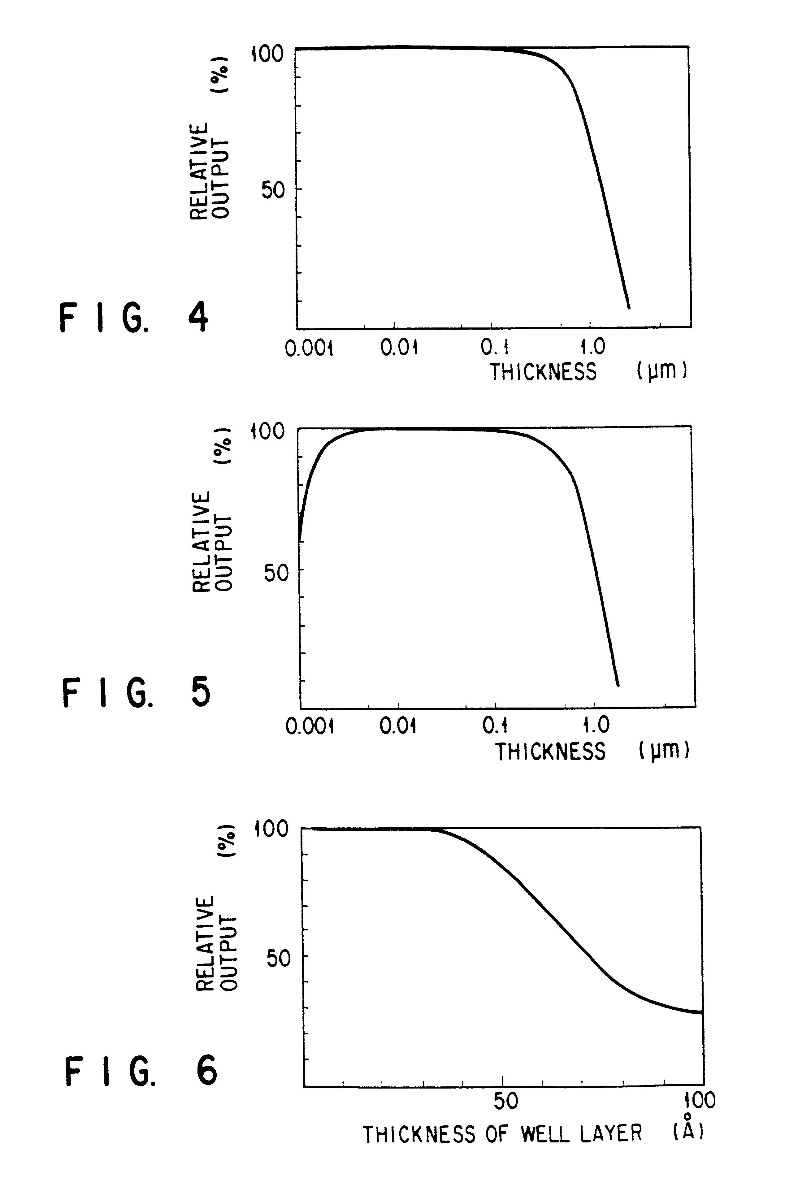
For example, when the thickness of the
Active layer is decreased to less than 200 angstroms, a large number of cracks are inevitably formed in the active layer and the clad layer, thus making it difficult to manufacture a light-emitting device.
This implies that since the clad
layers are inherently very hard in physical nature, it is impossible for the thin InGaN active layer to elastically alleviate an mismatching of the lattices at the interface as well as a difference in
thermal expansion coefficient between the active layer and the AlGaN clad layer.
Because of this
cracking in the clad layer and in the active layer, it has been impossible to make the active layer thinner.
However, since the active layer is always applied with strain due to a difference in
thermal expansion coefficient and due to the mismatching of
lattice constant, and since the thickness of the active layer of the conventional light-emitting device exceeds the
critical thickness enabling an elastic deformation of the active layer as mentioned above, the conventional active layer could not be elastically deformed, thus causing a large number of crystal defects in the active layer and making it impossible to emit a sufficient band-to-band emission.
On the other hand, if the carrier concentration is higher than 1.times.10.sup.19 / cm.sup.3, the crystallinity of the first p-type clad layer becomes deteriorated, thus possibly lowering the light-emitting efficiency.
On the other hand, if the carrier concentration is higher than 1.times.10.sup.19 / cm.sup.3, the crystallinity of the AlGaN becomes deteriorated, thus possibly lowering the light-emitting output.
If the carrier concentration is less than 5.times.10.sup.17 / cm.sup.3, the formation of
ohmic contact with an
electrode would become difficult, thus possibly making the Vf of the light-emitting device higher.
On the other hand, if the carrier concentration is higher than 5.times.10.sup.19 / cm.sup.3, the crystallinities of the n-type GaN as well as other nitride semiconductor
layers become deteriorated, thus possibly lowering the light-emitting efficiency.
If the carrier concentration is less than 1.times.10.sup.17 / cm.sup.3, the formation of
ohmic contact with an
electrode would become difficult.
On the other hand, if the carrier concentration is higher than 1.times.10.sup.19 / cm.sup.3, the crystallinities of the p-type GaN itself would become deteriorated, thus possibly lowering the light-emitting efficiency.
On the other hand, if the carrier concentration is higher than 1.times.10.sup.20 / cm.sup.3, the crystallinity of the first n-type clad layer becomes deteriorated, thus possibly lowering the light-emitting output.
On the other hand, if the carrier concentration is higher than 1.times.10.sup.19 / cm.sup.3, the crystallinity of the AlGaN becomes deteriorated, thus possibly lowering the light-emitting output.
On the other hand, if the carrier concentration is higher than 1.times.10.sup.19 / cm.sup.3, the crystallinity of the AlGaN becomes deteriorated, thus possibly lowering the light-emitting output.
By contrast, if a multi-layered film having a
total thickness of 0.5 .mu.m or more is to be formed using a plurality of AlGaN layers, each having a different
Al content from one another, cracks may be inevitably introduced in the multi-layered film, making it very difficult to prepare an intended device.
Because, as the
molar ratio of
indium is increased, the crystallinity of these InGaN tends to become more deteriorated, thus possibly lowering the light-emitting output.
However, if these clad layers are omitted, the emission output will be greatly diminished as compared with the case where these clad layers are not omitted.
When the conventional thick In.sub.z Ga.sub.1-z N is employed for the active layer, the resultant active layer would be poor in crystallinity.
For example, if the ratio of In, i.e., "z", is 0.3 to 0.5, the resultant crystal would become poor, exhibiting very
low emission output.

