Method for preparing layered perovskite compound thin film with organic ammonium layers and inorganic layers
a compound thin film and organic ammonium technology, applied in the direction of crystal growth process, polycrystalline material growth, after-treatment details, etc., can solve the problem that the method for preparing layered perovskite compound thin films has not been used successfully
- Summary
- Abstract
- Description
- Claims
- Application Information
AI Technical Summary
Benefits of technology
Problems solved by technology
Method used
Image
Examples
example 1
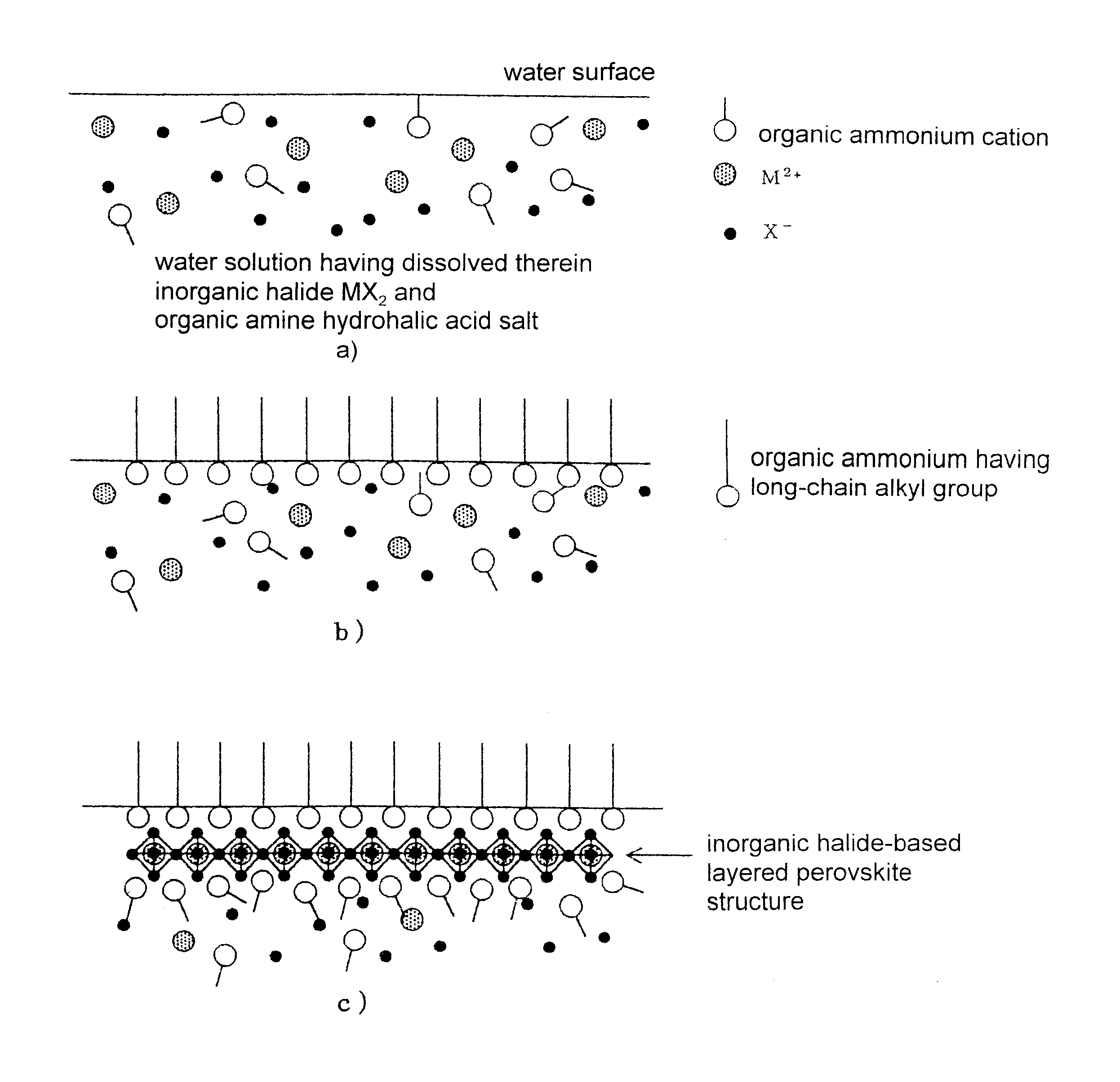
1.5 liters of water solution (concentration: 10.sup.-4 mol / l) having dissolved therein lead bromide as an inorganic halide MX.sub.2 and methylamine hydrobromide as an organic ammonium molecule was poured into a vessel and was kept in a stable state. Then, 2 ml of organic solvent solution (concentration: 10.sup.-4 mol / l) having dissolved therein dococylamine hydrobromide with chloroform as an organic solvent was dropped onto the surface of the water solution.
The organic solvent was completely evaporated just after the dropping. After the vaporization, when the monomolecular film was compressed to increase its surface pressure up to 30 mN.sup.-1, an organic-inorganic layered perovskite compound monolayer film of dococyl ammonium-lead bromide represented by the molecular formula (C.sub.22 H.sub.45 NH.sub.3).sub.2 PbBr.sub.4 was formed on the surface of the water solution. A fused quartz subjected to a hydrophobic treatment with hexamethyldisilazane was used as a substrate. The formed m...
example 2
An organic solvent containing about 10 volume % of dimethylformamide added in chloroform was used as a substitute for the chloroform used as an organic solvent in the example 1. Both of dococylamine hydrobromide C.sub.22 H.sub.45 NH.sub.3 Br and lead bromide are dissolved in the organic solvent to form an organic solvent solution to be used.
In this manner, a desired (C.sub.22 H45NH.sub.3).sub.2 PbBr.sub.4 layered perovskite thin film as in the example 1 could be prepared with excellent reproducibility. FIG. 3 shows an X-ray diffraction profile of a thin film formed through ten stack operations. A diffraction peak corresponding to (0 0 n) of the lead bromide-based layered perovskite was observed, and a layer pitch of 4.5 nm was calculated from the diffraction peak. This value matches with the layer pitch of the (C.sub.22 H45NH.sub.3).sub.2 PbBr.sub.4 layered perovskite. FIG. 4 conceptually shows the (C.sub.22 H45NH.sub.3).sub.2 PbBr.sub.4 layered perovskite structure.
example 3
A thin film was prepared in the same manner as that of the example 2 except for using CuBr.sub.2 as an inorganic halide. FIG. 5 shows an absorption spectrum of the obtained thin film. The absorption caused by d--d transition peculiar to copper bromide-based perovskite (C.sub.22 H45NH.sub.3).sub.2 CuBr.sub.4 was observed in the vicinity of each wavelength of 540 nm and 360 nm. This proves that a copper bromide-based layered perovskite thin film is obtained.
PUM
| Property | Measurement | Unit |
|---|---|---|
| volume % | aaaaa | aaaaa |
| wavelength | aaaaa | aaaaa |
| wavelength | aaaaa | aaaaa |
Abstract
Description
Claims
Application Information


