Silicon focus ring and method for producing the same

Inactive Publication Date: 2004-11-09
SHIN ETSU CHEM IND CO LTD
View PDF9 Cites 277 Cited by
  • Summary
  • Abstract
  • Description
  • Claims
  • Application Information

AI Technical Summary

Problems solved by technology

However, the graphite material is complex of particles consisting of aggregate and matrix, there may be problems such that constitutive particles are scattered and consumed due to plasma etching, and the particles fall on a silicon wafer to be treated, which may lead to trouble in formation of circuit pattern.
However, even if the glassy carbon is used for the focus ring, the silicon wafer can not be prevented from contamination.
In fabrication of a semiconductor device, contamination of a silicon wafer may cause to degrade its characteristics and lower device yield.
Even a small amount of such impurities cause a serious problem in fabrication process of a semiconduct

Method used


Image

  • Silicon focus ring and method for producing the same
  • Silicon focus ring and method for producing the same

Examples


example

Examples and Comparative examples will be explained below. (Examples 1 to 4, Comparative Examples 1 to 4)

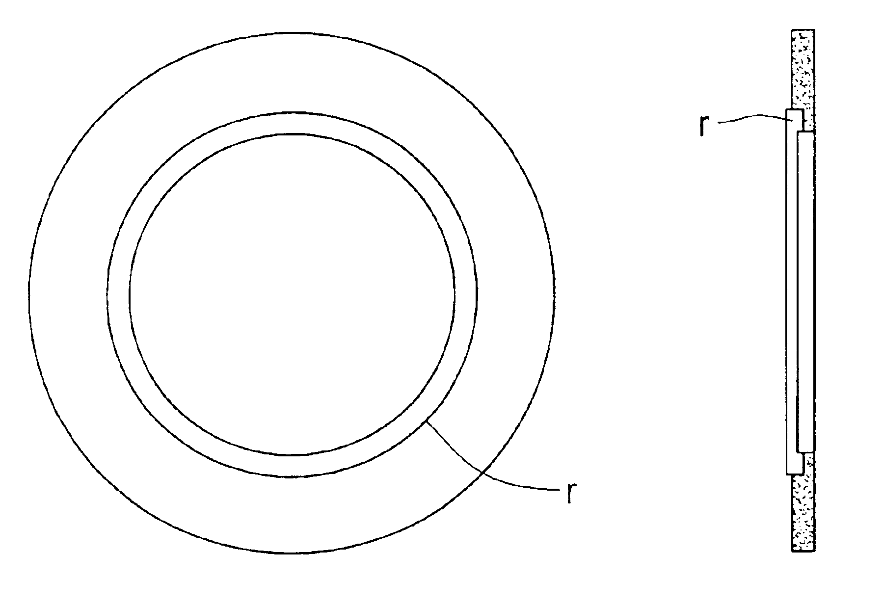
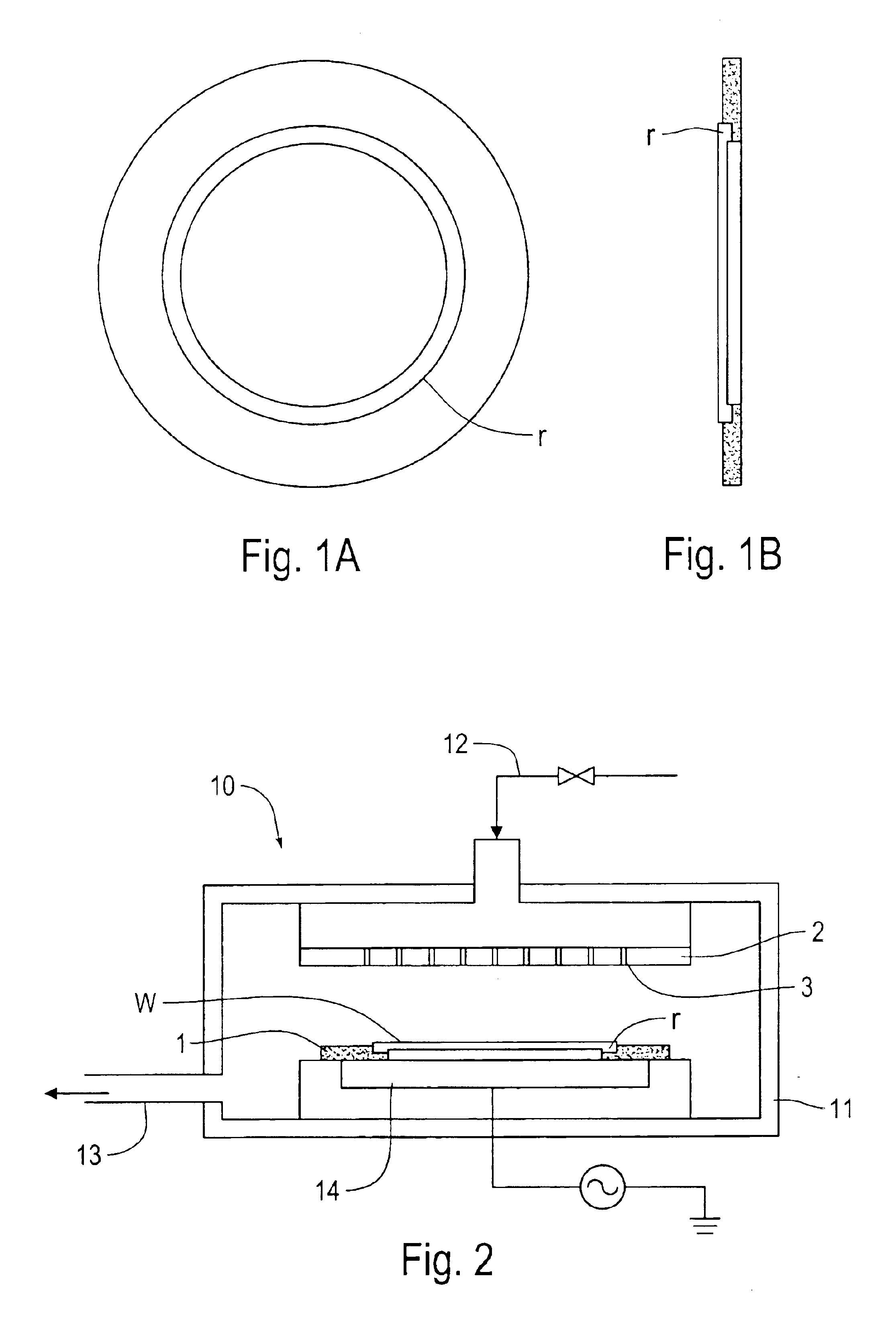
The silicon focus ring as shown in FIGS. 1(a) and (b) was produced by the following method.

In accordance with CZ method, polycrystalline silicon of raw material was charged into a quartz crucible having a diameter of 36 inches, and eight single crystal ingots of P type and 0.1 .OMEGA..multidot. cm having a diameter of 10 inches were pulled. Any of crystals were pulled with varying oxygen concentration in the single crystal by controlling the number of rotation of the crucible during pulling. Any of crystals were also pulled with varying nitrogen concentration in the single crystal by charging the silicon wafer having silicon nitride film of which thickness are different from each other in advance into the raw material.

The eight silicon single crystal ingots having a diameter of about 270 mm pulled as described above were subjected to a cylindrical grinding. Subsequently, the focu...


PUM


Abstract

There is disclosed a silicon focus ring consisting of silicon single crystal used as a silicon focus ring in a plasma apparatus, wherein concentration of interstitial oxygen contained in the silicon focus ring is not less than 5x10<17 >atoms/cm<3 >and not more than 1.5x10<18 >atoms/cm<3>, and a producing method for a silicon focus ring used for a plasma apparatus, wherein a single crystal silicon wherein concentration of interstitial oxygen contained in the silicon focus ring is not less than 5x10<17 >atoms/cm<3 >and not more than 1.5x10<18 >atoms/cm<3 >is grown by a Czochralski method, the single crystal silicon is processed in a circle, and a silicon focus ring is produced. There can be provided a silicon focus ring, which can prevent disadvantage due to impurities such as heavy metal.

Description

1. Field of the InventionThe present invention relates to a silicon focus ring for a plasma etching, for example, used for a dry etching apparatus used in a fabrication process of a semiconductor device.2. Description of the Related ArtFor example, in fabrication of such as a semiconductor device, apparatuses utilizing plasma are mostly used when a silicon wafer is formed thin film or etched. Among such apparatuses, for example, when a parallel plate plasma apparatus is used, a silicon wafer to be treated is placed on a lower electrode side, a reaction gas is distributed from an upper electrode side, which is parallel to the lower electrode, and high frequency plasma is generated by applying high frequency voltage to both electrodes, so that the silicon wafer can be etched.As for such a plasma apparatus, in order to maintain even characteristics of a semiconductor device to be fabricated on the surface of a silicon wafer, plasma supplied to a silicon wafer has to be uniformed. There...

Claims


Application Information

Patent Timeline
IPC IPC(8): C30B29/06H01L21/02H01L21/302H01L21/3065H05H1/46C30B15/00H01J37/32
CPCC30B15/00H01J37/32642C30B29/06H01L21/3065
Inventor TAMURA, KAZUYOSHIKAWAI, MAKOTOGOTO, KEIICHI
Owner SHIN ETSU CHEM IND CO LTD
Why Eureka
Try Eureka