

Avalanche photodiode for use in harsh environments
a photodiode and harsh environment technology, applied in the field ofavalanche photodiodes, can solve the problems of increasing the cost of use, affecting the accuracy of measurement results, and prone to failure,
- Summary
- Abstract
- Description
- Claims
- Application Information
AI Technical Summary
Benefits of technology
Problems solved by technology
Method used
Image

Examples
Embodiment Construction
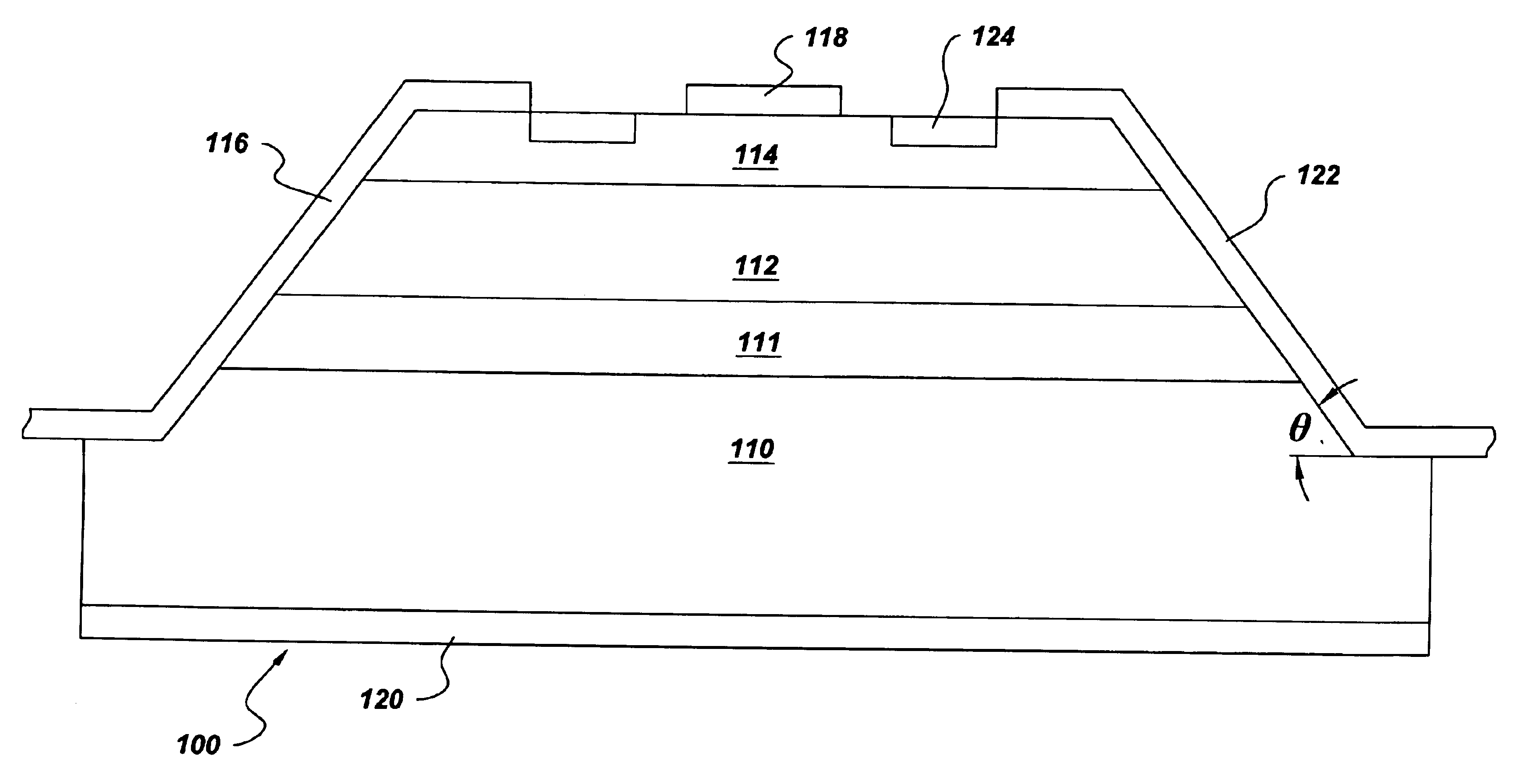
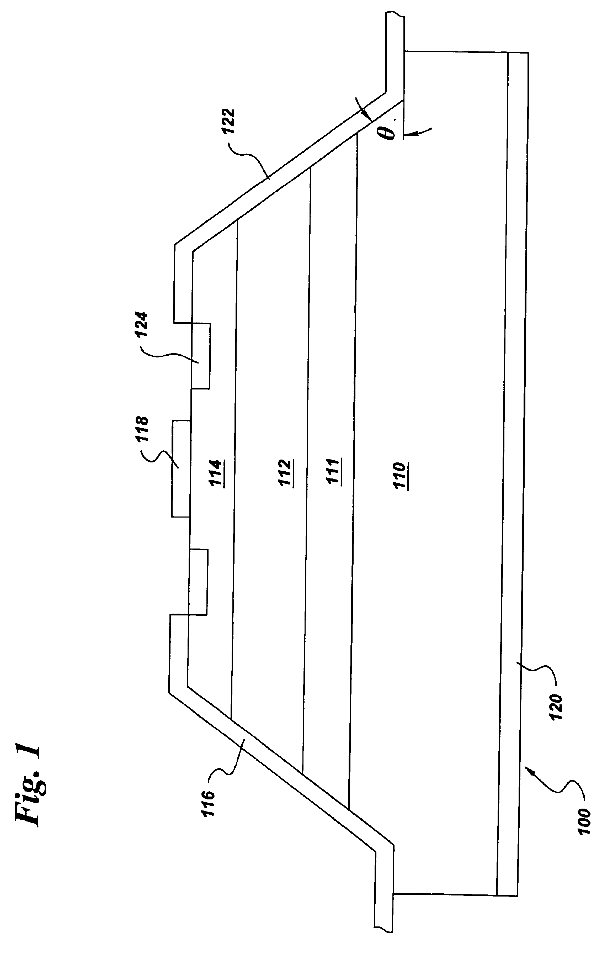
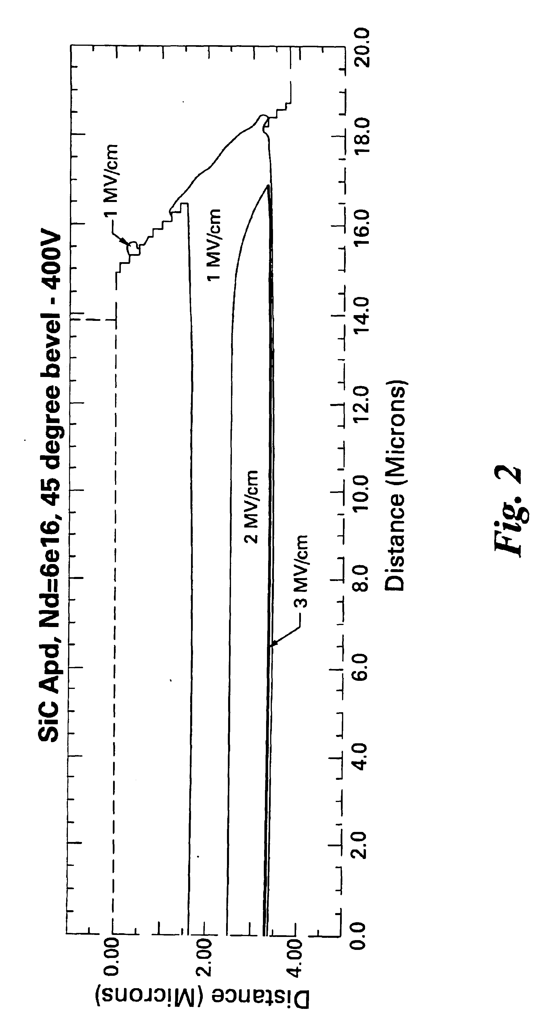
An aspect of the present invention is directed to an avalanche photodiode (APD) device for use in oil well drilling applications in harsh, down-hole environments where shock levels are near 250 gravitational acceleration (G) and / or temperatures approach or exceed 150° C. Another aspect of the present invention is directed to an APD device fabricated using SiC materials. Another aspect of the present invention is directed to an APD device fabricated using GaN materials. An avalanche photodiode is a photodiode that operates with a reverse bias voltage that causes a primary photocurrent to undergo amplification by cumulative multiplication of charge carriers. As the reverse-bias voltage increases toward a breakdown, hole-electron pairs are created by absorbed photons. An avalanche effect occurs when the hole-electron pairs acquire sufficient energy to create additional pairs of holes and electrons, thereby achieving a signal gain.
PUM
 Abstract
Description
Claims
Application Information