Multi-layer dispersion-engineered waveguides and resonators

a multi-layer dispersion engineered waveguide technology, applied in the field of optical waveguides and resonators, can solve the problems of unwanted phase and/or frequency modulation, adds significantly to the cost, size and power consumption of any fiber-optic system or sub-system, and cannot realize the full potential of powerful new on-chip integrated optical devices. , to achieve the effect of a larger modal index shi

Inactive Publication Date: 2005-01-04
HOYA USA
View PDF21 Cites 34 Cited by
  • Summary
  • Abstract
  • Description
  • Claims
  • Application Information

AI Technical Summary

Benefits of technology

One or more of the foregoing objects may be achieved in the present invention by an optical waveguide/resonator including at least one multi-layer laterally-confined dispersion-engineered optical waveguide segment. The multi-layer waveguide segment may include a single multi-layer reflector stack for guiding a surface-guided optical mode (SGOM). The multi-layer waveguide segment may also include lateral lower-index portions thereof for lateral confinement of the surface-guided optical mode, and may include a waveguide or core layer thereon. The multi-layer waveguide segment may further comprise one or more electro-active and/or non-linear-optical layers and control components for controlling the refractive index and/or optical loss thereof. Strongly dispersive optical properties of the single-reflector-guided SGOM (a substantially flat dispersion relation in the operating wavelength range, so that a narrow range of wavelengths cover a wide range of propagation constants or modal indices) serve to produce a substantially larger modal index shift of the SGOM for a given applied control signal than previous devices. The surface-guided optical mode may be transverse-coupled to another optical mode of another optical element. Control of the modal index and/or optical loss may enable control of: optical power transfer between the waveguide/resonator and another optical element; the resonance frequency of a resonant optical mode of a resonator; and an operatio...

Problems solved by technology

Direct intensity modulation of the light source (usually a laser diode) generally induces unwanted phase and/or frequency modulation as well, which may be problematic when the modulated optical mode must propagate long distances within the optical fiber, or when the modulated optical mode is one narrow-linewidth wavelength component among many within a wavelength division multiplexed (WDM) fiber-optic telecommunication system.
High insertion losses associated with currently available devices necessitate use of optical amplifiers to boost optical signal levels in a fiber-optic telecommunications system, essentially to replace optical power thrown away by the use of lossy modulators, couplers, and other devices.
This adds significantly to the cost, size, and power consumption of any fiber-optic system or sub-system.
Furthermore, the full potential of powerful new on-chip integrated optical devices cannot be realized when a substantial fraction of the optical signal is lost through inefficient transfer of optical power between an optical fiber and a waveguide on an integrated optical chip.
The relatively high Vπ of typical lithium niobate modulators forces the use of expensive high speed electronic drivers (described below), increasing...

Method used


Image

  • Multi-layer dispersion-engineered waveguides and resonators
  • Multi-layer dispersion-engineered waveguides and resonators
  • Multi-layer dispersion-engineered waveguides and resonators

Examples


Embodiment Construction

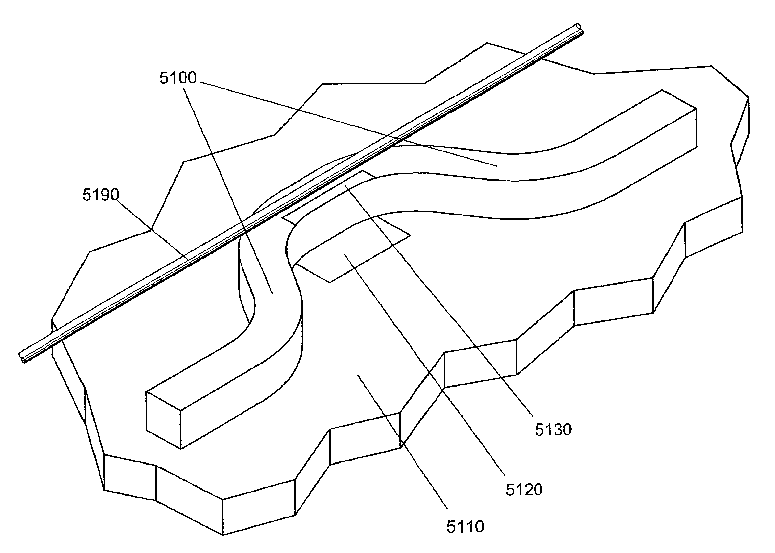
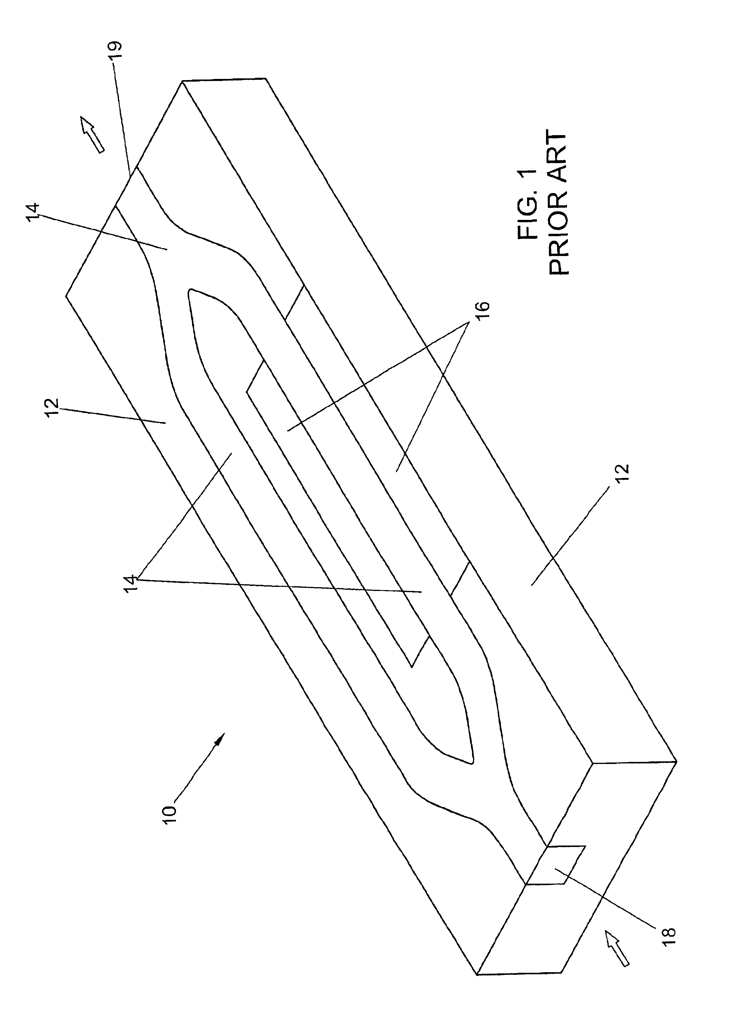
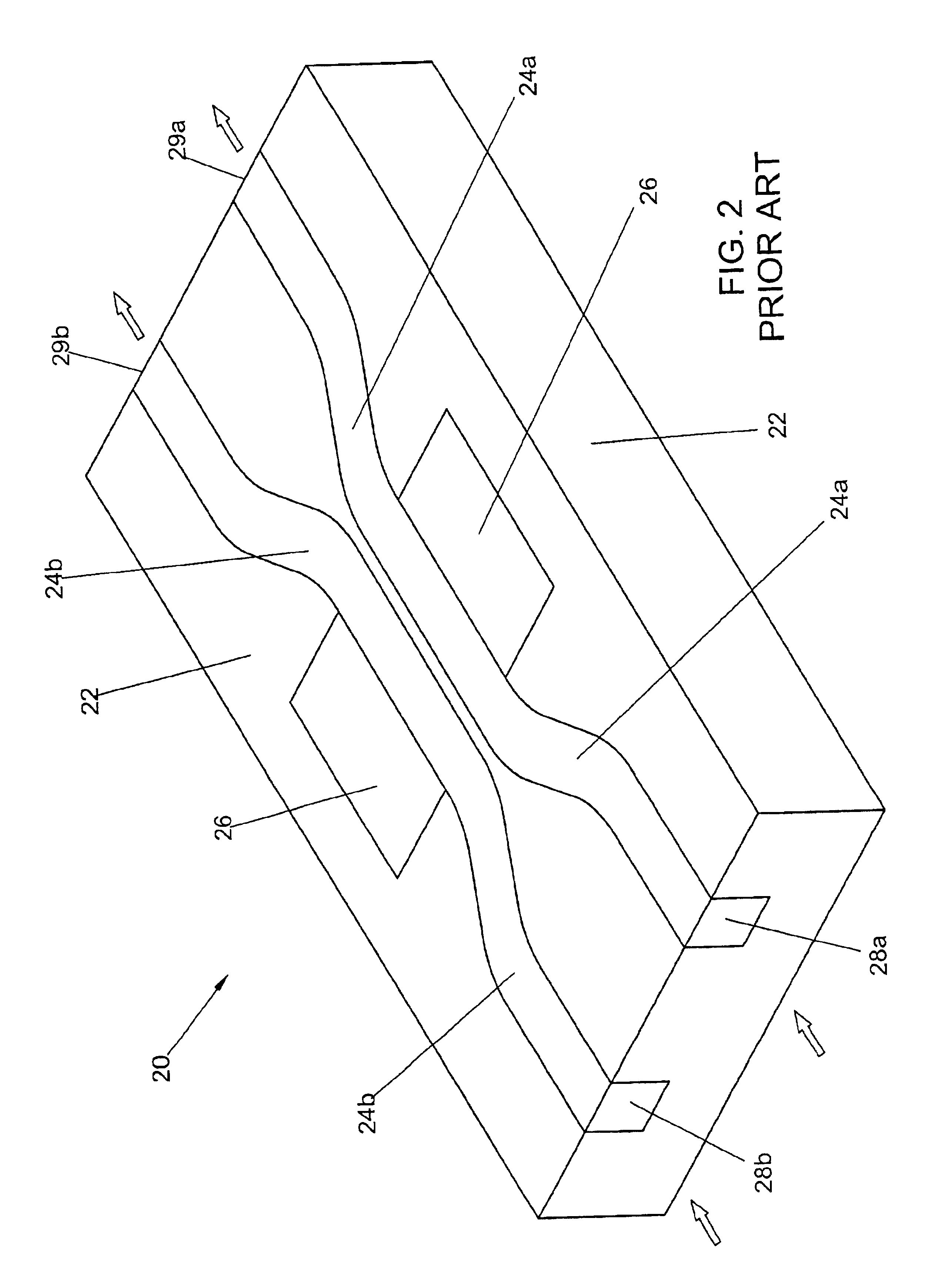
For purposes of the present written description, the term “waveguide” shall often be intended encompass both open waveguides (in which no closed optical path is provided for allowing re-circulation of optical power within an optical mode supported by the waveguide) and closed waveguides (in which a closed optical path is provided for allowing re-circulation of optical power within an optical mode supported by the waveguide; such closed waveguides may also be equivalently referred to as resonators or rings). The term “waveguide” shall often be used herein to denote both open and closed structures when structure and / or fabrication of such open and closed waveguides is discussed. In portions of the written description wherein only one or the other type of waveguide (open or closed) is described, it will be made clear in the text which is intended, either implicitly or explicitly. This will typically be the case when functional aspects of devices incorporating the open and / or closed...


PUM


Abstract

A multi-layer laterally-confined dispersion-engineered optical waveguide may include one multi-layer reflector stack for guiding an optical mode along a surface thereof, or may include two multi-layer reflector stacks with a core therebetween for guiding an optical mode along the core. Dispersive properties of such multi-layer waveguides enable modal-index-matching between low-index optical fibers and/or waveguides and high-index integrated optical components and efficient transfer of optical signal power therebetween. Integrated optical devices incorporating such multi-layer waveguides may therefore exhibit low (<3 dB) insertion losses. Incorporation of an active layer (electro-optic, electro-absorptive, non-linear-optical) into such waveguides enables active control of optical loss and/or modal index with relatively low-voltage/low-intensity control signals. Integrated optical devices incorporating such waveguides may therefore exhibit relatively low drive signal requirements.

Description

FIELD OF THE INVENTIONThe field of the present invention relates to devices for modulating, routing and / or processing optical signal power transmission. In particular, optical waveguides and resonators for integrated optical devices, as well as methods of fabrication and use thereof, are disclosed herein. The waveguides and resonators include a multi-layer laterally-confined dispersion-engineered waveguide segment, and may further include one or more active layers, thereby enabling tailoring of optical properties of the waveguide / resonator, and / or controlled modulation thereof.BACKGROUNDThis application is related to subject matter disclosed in:A1) U.S. provisional Application No. 60 / 111,484 entitled “An all-fiber-optic modulator” filed Dec. 7, 1998 in the names of Kerry J. Vahala and Amnon Yariv, said provisional application being hereby incorporated by reference in its entirety as if fully set forth herein;A2) U.S. application Ser. No. 09 / 454,719 entitled “Resonant optical wave po...

Claims


Application Information

Patent Timeline
IPC IPC(8): G02F1/01G02B6/13G02B6/132G02B6/10G02B6/122G02F1/29G02B6/12G02B6/34G02F1/225G02F1/313G02B6/30G02F1/017G02B6/26
CPCB82Y20/00G02B6/12007G02B6/122G02B6/132G02B6/30G02F1/0118G02F1/225G02F1/3137G02B6/10G02F2203/15G02B6/266G02B2006/12097G02B2006/12128G02B2006/12142G02B2006/12145G02B2006/12147G02B2006/12159G02B2006/12176G02F1/011G02F1/01708G02F2201/063G02F2201/307
Inventor PAINTER, OSKAR J.VERNOOY, DAVID W.VAHALA, KERRY J.
Owner HOYA USA
Why Eureka
Try Eureka