Interchangeable CML/LVDS data transmission circuit

a data transmission circuit and cml technology, applied in logic circuit coupling/interface arrangement, pulse technique, baseband system details, etc., can solve the problems of many dc biasing problems, large noise cancellation, and high jitter requirements for transmission of such fast signals, so as to improve the speed of switching transistors and speed up the operation. the effect of the predrive stage and the ability to swing more quickly

Inactive Publication Date: 2005-01-25
TEXAS INSTR INC
View PDF6 Cites 66 Cited by
  • Summary
  • Abstract
  • Description
  • Claims
  • Application Information

AI Technical Summary

Benefits of technology

An advantage of the present invention is that the use of a smaller (e.g., 1V P—P) input voltage from the predrive circuit, allows faster operation of the switching transistors of the current mode switch circuit. The lower input voltage swing means that not as much charge current must be dumped in and out of the gate oxide region as with prior art MOS drives, therefore the voltage is allowed swing more quickly.
Another related advantage of the present invention comes through using MOS transistors as drive elements for the simplification of the predrive stage. Since MOS transistors have a much larger range of DC input voltages over which they are able to work effectively, the predrive circuit is not required to maintain an extremely tight common mode range.
Still another advantage of the present invention, is in the use of bipolar (e.g., NPN) transistors in the voltage mode output circuit (e.g., first output drive portion), which allows a simple voltage follower design configuration in combination with the compensation circuit, while providing a very high current gain for the voltage regulation of the common mode voltage.
To the accomplishment of the foregoing and related ends, the invention comprises the features hereinafter fully described and particularly pointed out in the claims. The following description and the annexed drawings set forth in detail certain illustrative embodiments of the invention. These embodiments are indicative, however, of but a few of the various ways in which the principles of the invention may be employed. Other objects, advantages and novel features of the invention will become apparent from the following

Problems solved by technology

This enables noise to travel at the same level as the signal, but common to both wires (common mode), causing the vast majority of the noise to cancel.
Physical layer interfaces are often a critical bottleneck in an application that requires high bandwidths, such as telecommunications and high speed networking.
One of the chief technical problems in producing a high speed repeater (e.g., up to 1.36 Gbps operation desired by many telecommunications customers) is meeting the extremely low rise / fall time and jitter requirements necessary for transmission of such fast signals.
Though Bipolar circuits are fast, many DC biasing problems arise in the predrive and common mode correction schemes which are required to support these circuits.
This conventional circuit has provided years of excellent results in LVDS systems, but can only achieve rise and fall times in the 400 ps range.
The first problem is in the biasing of the predrive signals.
This type of control is difficult to achieve, and requires a great deal of care on the part of the designer.
The second problem is that of common mode control.
The topology of the driver output stage 350 is such that any control of the common mode is difficult at best, and probably will not meet the stringent requirements of the TIA / EIA644 standard.
Outputs of this type are generally not tri-stateable, and there is no standard for short circuit protection or leakage current, etc.

Method used


Image

  • Interchangeable CML/LVDS data transmission circuit
  • Interchangeable CML/LVDS data transmission circuit
  • Interchangeable CML/LVDS data transmission circuit

Examples


Embodiment Construction

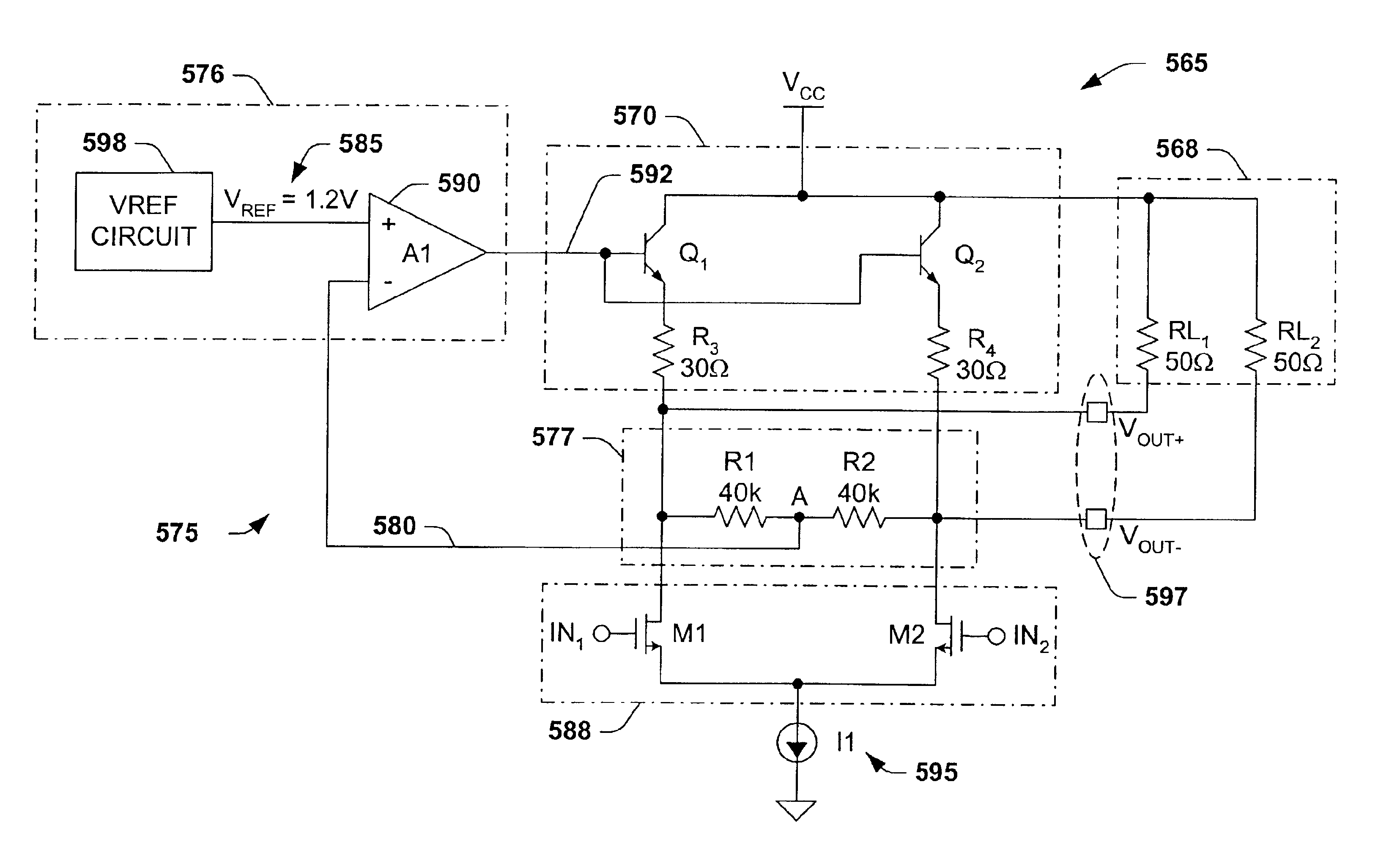
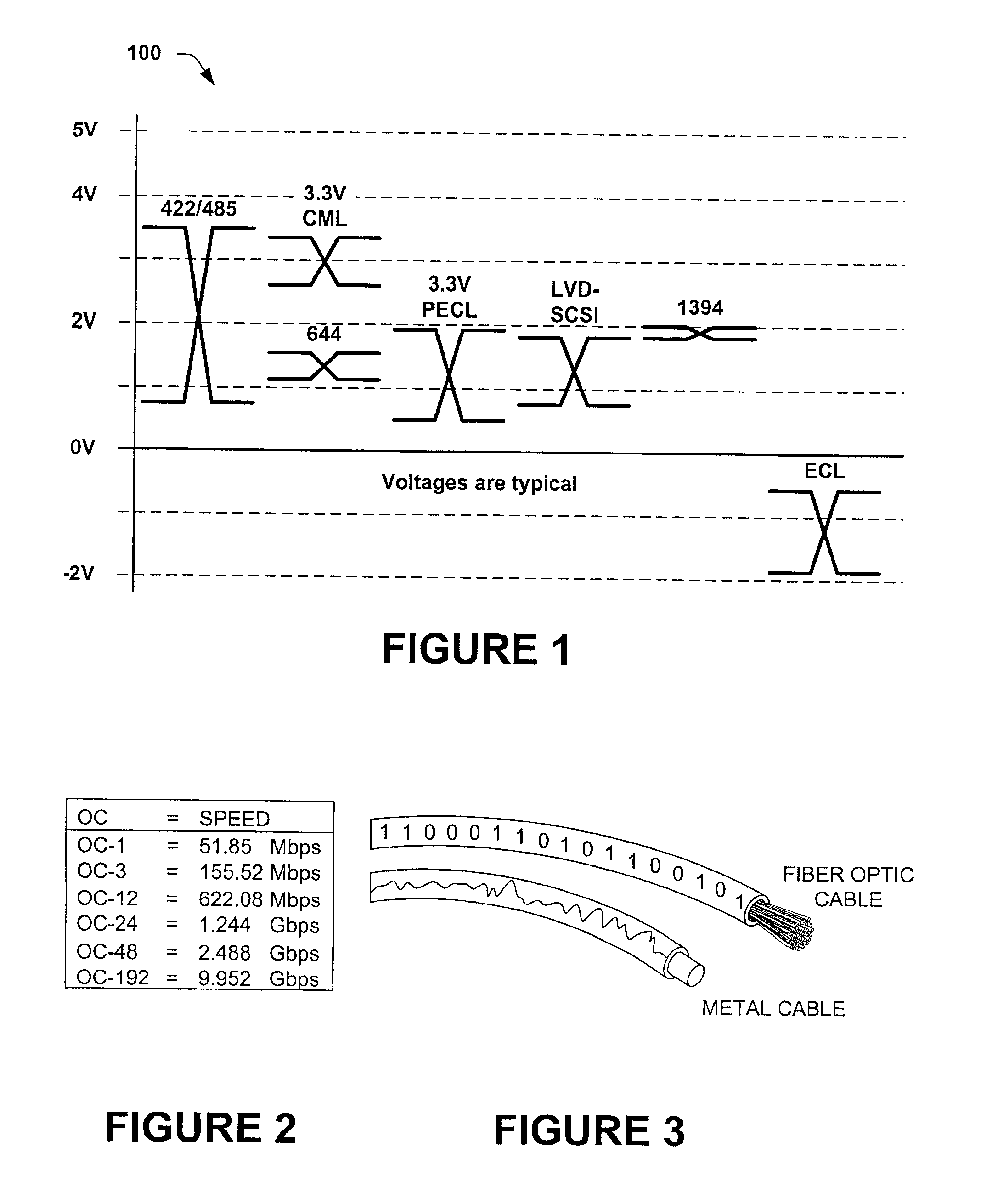
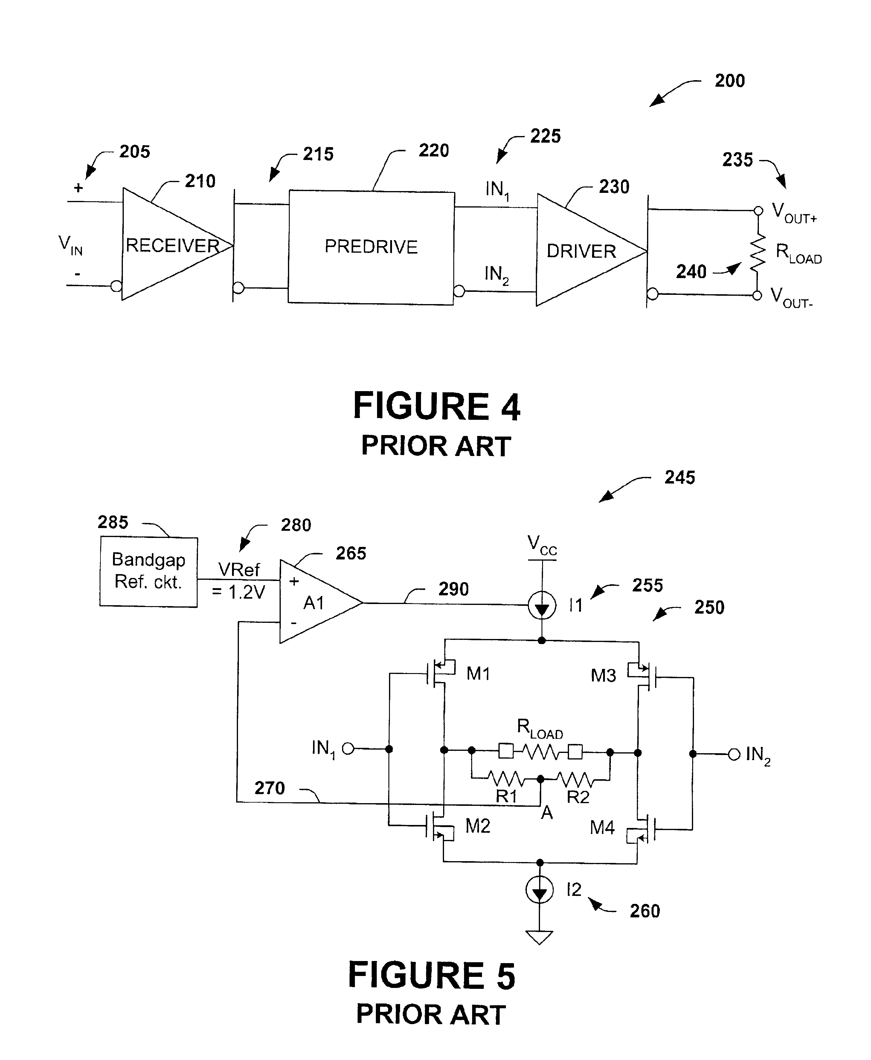
The present invention will now be described with reference to the drawings, wherein like reference numerals are used to refer to like elements throughout. The present invention relates to a high speed driver circuit used in the field of telecommunications, and for data communications transmission in LVDS transceiver device applications (e.g., LVDS repeaters and PECL / ECL to LVDS converters), and CML transceiver device applications (e.g., on PCB transmitters and receivers). The transceivers are intended to receive a low voltage differential input signal and interchangeably drive a standard LVDS load with a TIA / EIA-644 compliant LVDS signal, or a standard CML load with a standard CML compatible signal. The driver circuit operates at speeds up to 1.36 Gbps, making it compatible with the OC-24 signaling rate for optical transmission.

The high speed driver circuit employs the use of a mixed voltage mode and a current mode drive section in the output circuit when coupled to LVDS loads, and ...


PUM


Abstract

A system and method is described for a driver circuit used for high speed data transmission in LVDS and CML transceiver device applications. The transceivers are intended to receive a low voltage differential input signal and interchangeably drive a standard LVDS load with a TIA/EIA-644 compliant LVDS signal, and a standard CML load with a standard CML compatible signal. The driver circuit operates at speeds up to 1.36 Gbps, making it compatible with the OC-24 signaling rate for optical transmission. To accomplish this, the driver uses a mixed combination of voltage and current mode drive sections in the output circuit when coupled to LVDS loads, and when the driver is coupled to CML loads, operates purely in a current mode using only the current mode drive section. MOS transistors and a current source are used in the current mode switch portion to switch the drive with a constant current at the high speeds, and NPN transistors in the voltage mode output portion provide variable impedance for the output circuit. A common mode compensation circuit using a feedback voltage from the load generates a compensation signal for variable impedance control of the NPN transistors to yield a regulated voltage for the common mode dc voltage.

Description

TECHNICAL FIELD OF INVENTIONThe present invention relates generally to transceiver device applications in the transmission of CML and LVDS level signals. More particularly, the present invention relates to a high speed driver circuit for data transmission of a standard CML or a standard LVDS compatible differential signal, providing high compliance of the common mode output even at high load currents, while maintaining a simple pre-drive circuit design with a wide common mode range.BACKGROUND OF THE INVENTIONLow Voltage Differential Signaling (LVDS) and Current Mode Logic (CML) standards are two of the most common high-speed data transmission methods used today, and are redefining data transmission at the physical layer interface, and the point-to-point device interface. LVDS and CML are bringing high speeds and low power to these critical interfaces, providing an essential step in meeting the high bandwidth requirements of tomorrow's networking, telecommunications and multimedia ap...

Claims


Application Information

Patent Timeline
Patent Type & Authority Patents(United States)
IPC IPC(8): H03K19/0175H03K19/0185H04L25/02
CPCH03K19/017527H03K19/018585H04L25/0274H04L25/028H04L25/0292H04L25/0294H04L25/0282H04L25/0278H03F3/45183
Inventor TINSLEY, STEVENDIETZ, JAMESMORGAN, MARK
Owner TEXAS INSTR INC
Why Eureka
Try Eureka