

Highly selective process for etching oxide over nitride using hexafluorobutadiene
a technology of etching oxide and nitride, which is applied in the direction of decorative surface effects, electrical appliances, decorative arts, etc., can solve the problems of increasing the number of devices on the chip, increasing the difficulty of etching, and increasing the minimum feature size, so as to improve the quality of the polymer, the effect of high selectivity to nitride and reducing power levels
- Summary
- Abstract
- Description
- Claims
- Application Information
AI Technical Summary
Benefits of technology
Problems solved by technology
Method used
Image

Examples
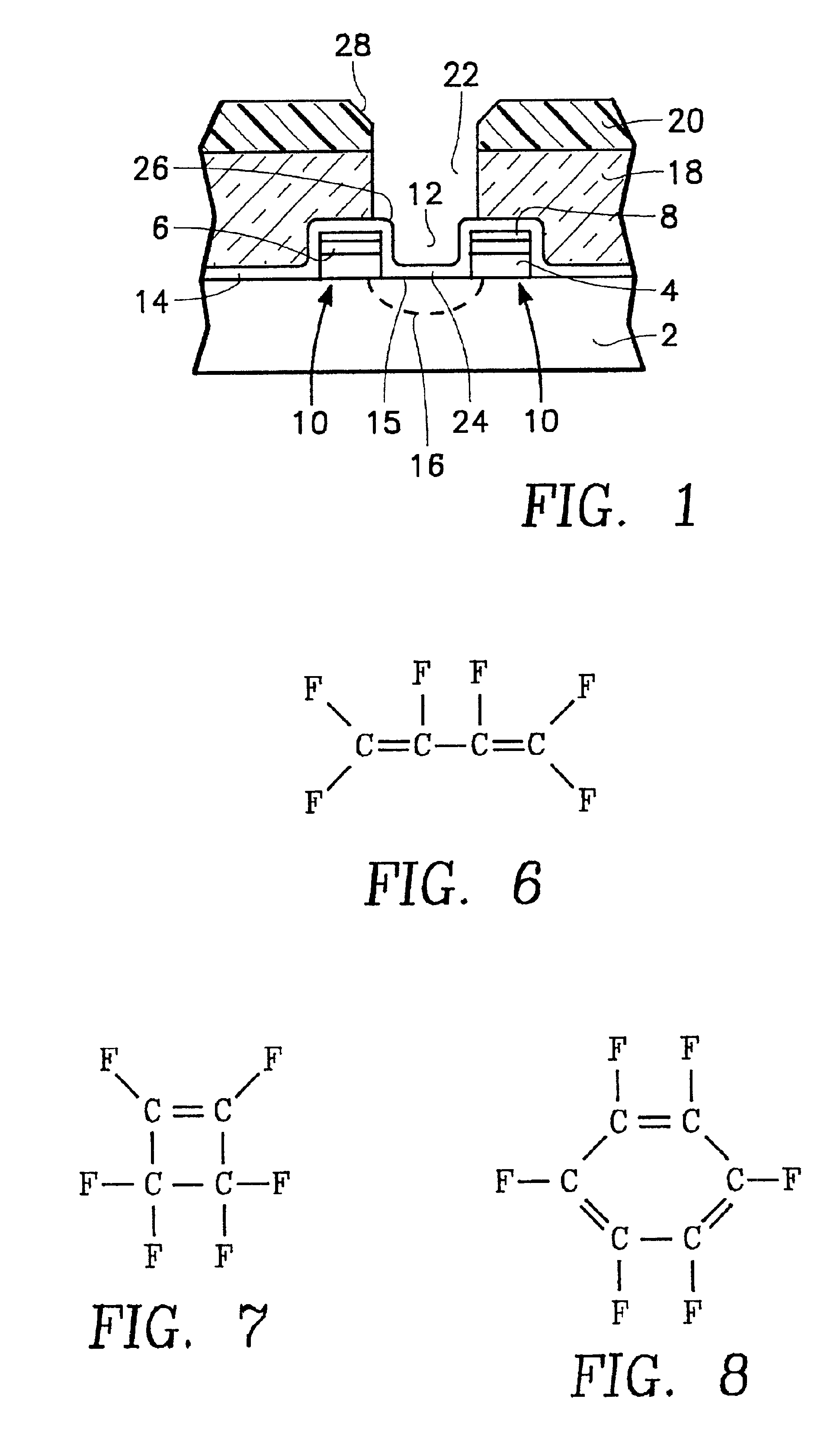
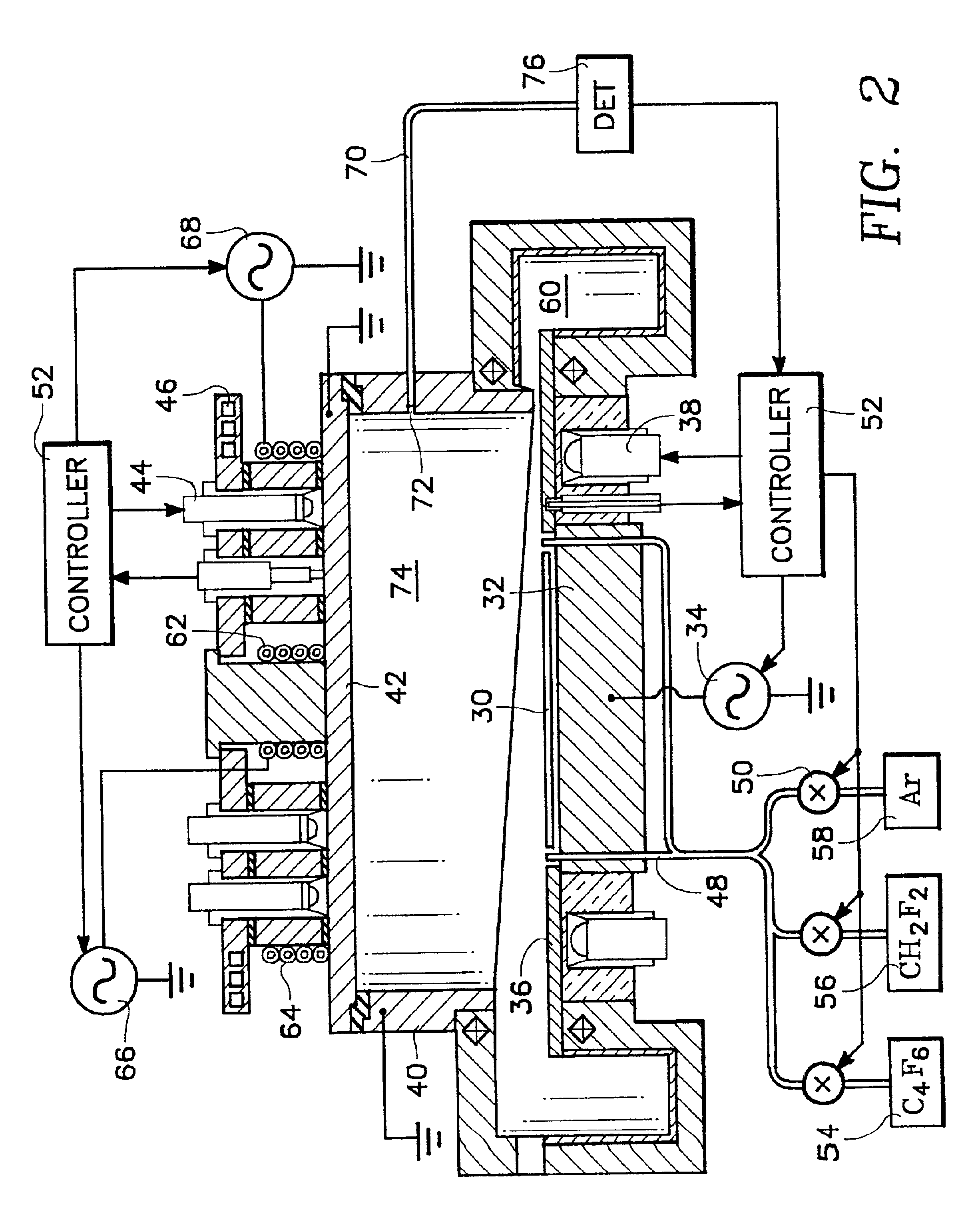
first embodiment
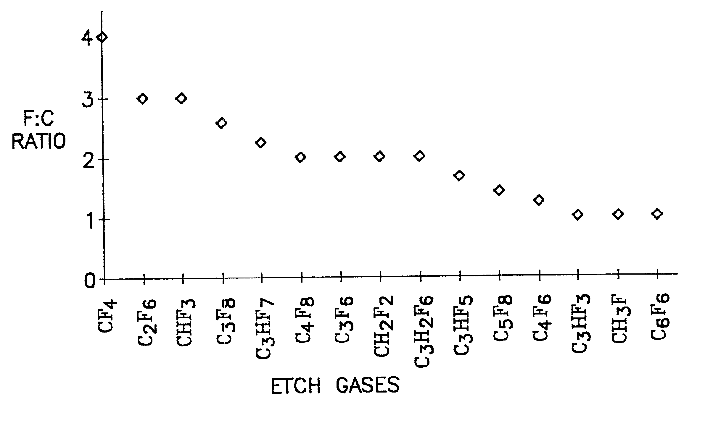
the two-step etch recipe including an additive gas is summarized in TABLE 7.
TABLE 7MainOverEtchEtchC4F6 Flow (sccm) 20 20CH2F2 Flow (sccm) 0 10Ar Flow (sccm)100100Inner Source Power (W) 0 0Outer Source Power (W)1600 1600 Bias Power (W)1400 1400 Pressure (mTorr) 10 10Roof Temp. (° C.)230230Ring Temp. (° C.)300300Cathode Temp. (° C.)+15+15Backside He Pressure 7 7(Torr)Time (s)100 30
This recipe was applied to the second, tall SAC structure. The profile angle in the oxide portion of the hole is observed to be at least 87°, and the nitride selectivity is acceptable.
The timing of the switch between the main etch and the over etch is chosen such that the main etch reaches the nitride bottom at most of the locations on the wafers and the over etch guarantees a complete etch without producing excessive nitride faceting. To provide further nitride protection, the changeover can be moved to a point where the main etch has passed the top of the nitride at most locations, that is, is somewhere i...
PUM
| Property | Measurement | Unit |
|---|---|---|
| Temperature | aaaaa | aaaaa |
| Magnetic field | aaaaa | aaaaa |
| Flow rate | aaaaa | aaaaa |
Abstract
Description
Claims
Application Information