Laser irradiation apparatus, laser irradiation method, and method of manufacturing a semiconductor device

a laser irradiation and semiconductor technology, applied in metal working apparatus, transistors, manufacturing tools, etc., can solve the problems of fluctuation among tfts on the same substrate, and achieve excellent uniformity of energy distribution, lightening of weight, and enhancing durability or the like

Inactive Publication Date: 2005-02-08
SEMICON ENERGY LAB CO LTD
View PDF28 Cites 39 Cited by
  • Summary
  • Abstract
  • Description
  • Claims
  • Application Information

AI Technical Summary

Benefits of technology

Moreover, in the configurations described above, it is preferable to use a film containing silicon for the foregoing semiconductor film. For the foregoing substrate forming the semiconductor film, a glass substrate, a quartz substrate, a silicon substrate, a plastic substrate, a metal substrate, a stainless clad substrate, a flexible substrate and the like can be utilized. As the foregoing glass substrate, a substrate consisted of glass such as barium borosilicate glass, aluminum borosilicate glass or the like can be listed. Moreover, a flexible substrate is referred to a substrate in a film shape consisted of PET, PES, PEN, acryl or the like, if a semiconductor device is prepared by utilizing the flexible substrate, the weight lightening of it is expected. If on the surface or on the surface and the back surface of the flexible substrate, a barrier layer made of aluminum film (AlON, AlN, AlO or the like), carbon film (DLC (diamond like carbon) or the like), SiN or the like is formed in a monolayer or multilayer, it is desirable that the durability or the like is enhanced.
In the present invention, laser light very excellent in uniformity of energy distribution can be formed on an irradiation surface or in the vicinity thereof by using the plural laser lights having the attenuation regions. And accordingly, an object to be irradiated can be annealed uniformly by using such kind of laser light. Moreover, since the attenuation regions where energy density has being insufficient for performing annealing up to now is utilized effectively, throughput can be enhanced. Further, since a semiconductor film formed on the substrate can be irradiated effectively and uniformly, the crystallization and crystallinity of the semiconductor film can be improved, and the activation of the impurity elements can be performed well. Furthermore, the dispersion of electric properties of the obtained TFT by using such a semiconductor film can be reduced, thereby good electric properties obtaining. Moreover, a semiconductor device manufactured by such TFTs, operation properties and reliabilities thereof can be improved.

Problems solved by technology

In comparison with the central part of the laser light, the energy density in the attenuation regions is not enough, for this reason, an object to be irradiated cannot be annealed sufficiently by using the laser light having the attenuation regions.
Therefore, if this semiconductor film is used to manufacture TFTs, the electric characteristic of a TFT formed from the region that is annealed by the attenuation region is inferior to other TFTs and causes fluctuation among the TFTs on the same substrate.

Method used


Image

  • Laser irradiation apparatus, laser irradiation method, and method of manufacturing a semiconductor device
  • Laser irradiation apparatus, laser irradiation method, and method of manufacturing a semiconductor device
  • Laser irradiation apparatus, laser irradiation method, and method of manufacturing a semiconductor device

Examples


embodiment 1

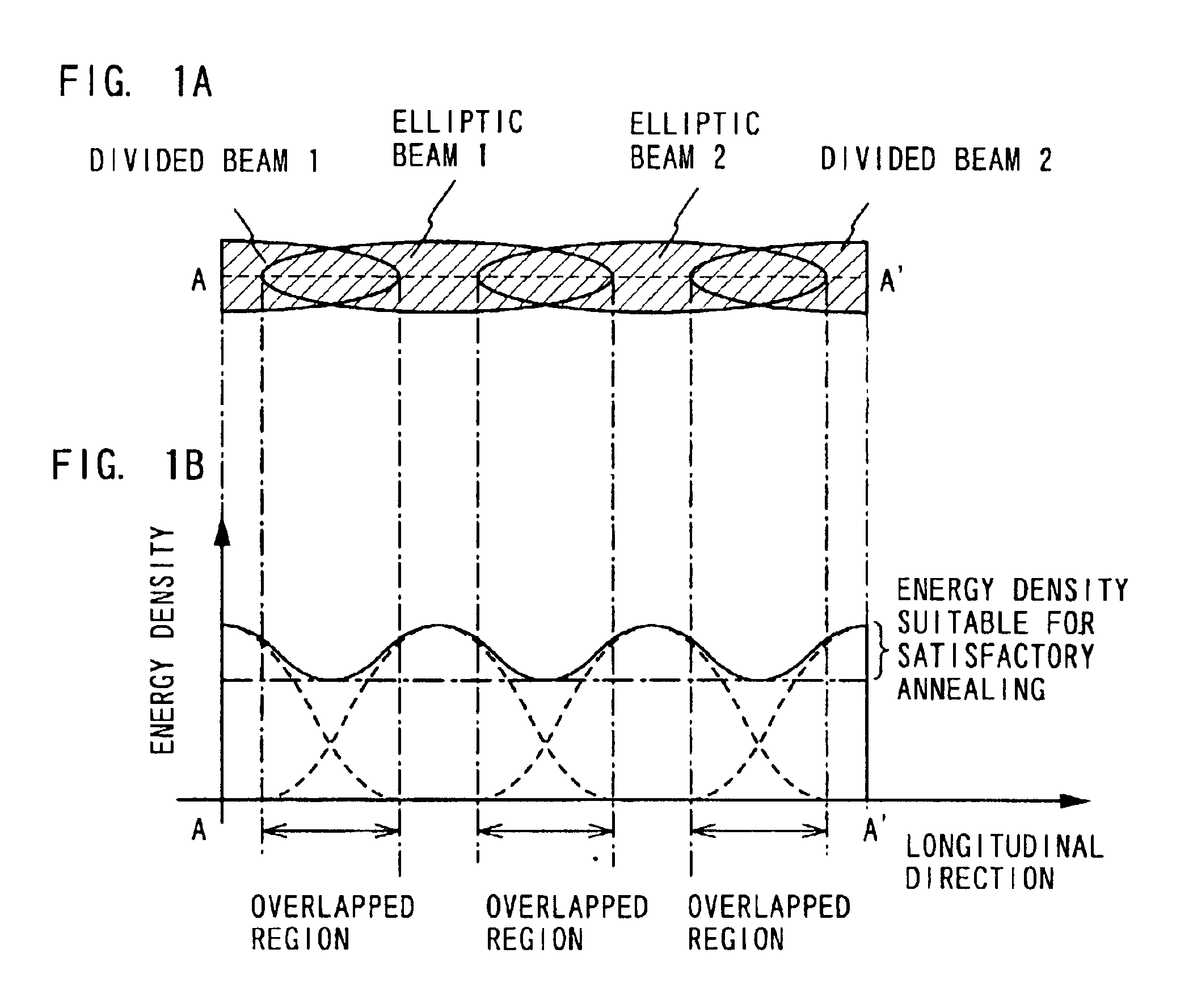
This embodiment gives a description on energy density suitable for annealing in the present invention with reference to FIG. 19.

FIG. 19 is the simulation result of energy density distribution when one of laser beams emitted from three lasers is divided and attenuation regions of the divided laser beams are synthesized with attenuation regions of other laser beams as shown in FIGS. 1A to 1B. The lasers used here are YAG lasers and laser beams emitted from the lasers are converted into the second harmonic by LBO crystals. The beam diameter of the laser light is set to 2.25 mm (1 / e2 width) and the TEM∞ mode is employed. In FIG. 19, the dotted line indicates the energy density in the longitudinal direction and the solid line indicates the energy density in the lateral direction.

FIG. 19 shows that distribution of the energy density in the longitudinal direction is within ±10% of the average of the energy density except for attenuation regions. A region with crystals of large diameters ca...

embodiment 2

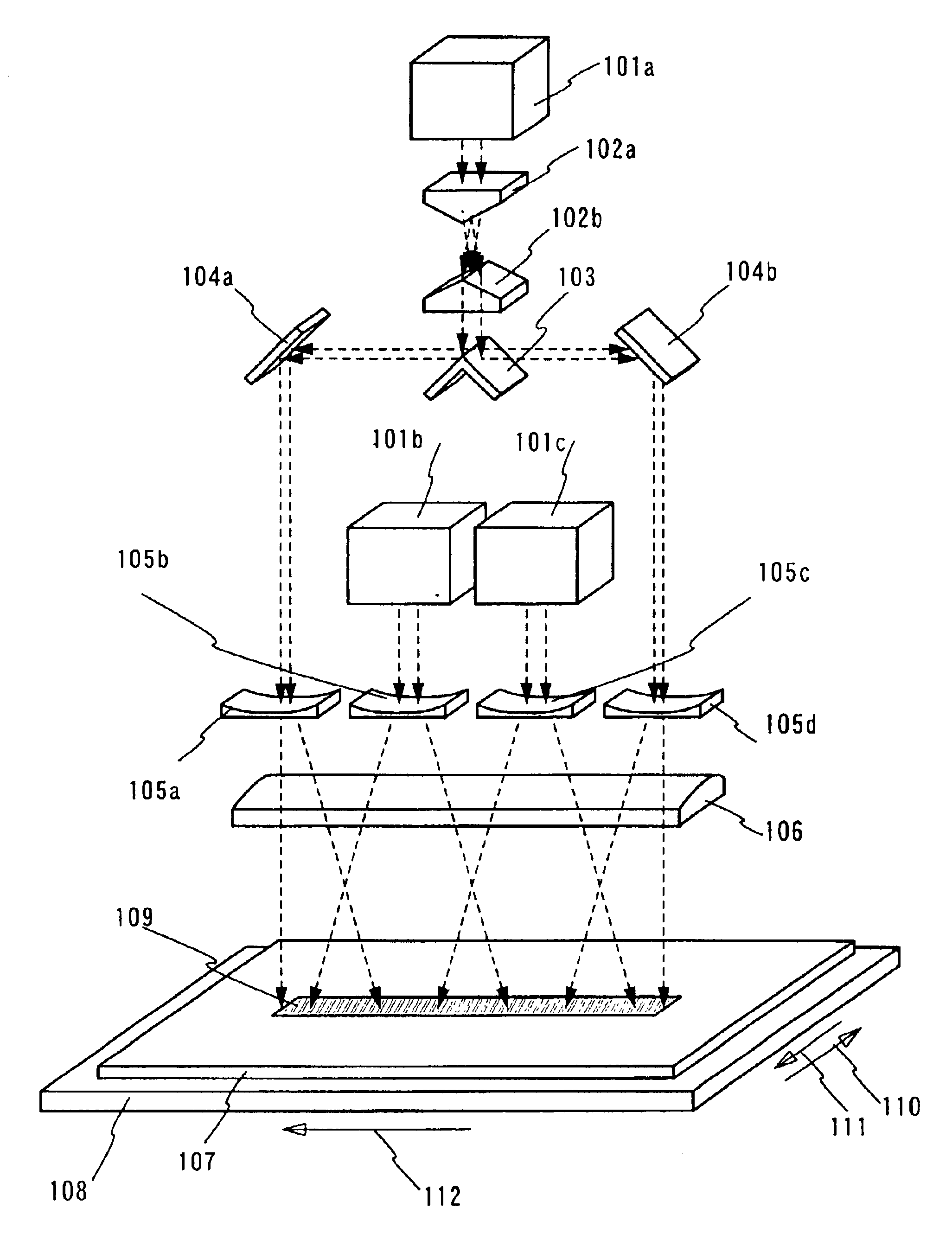
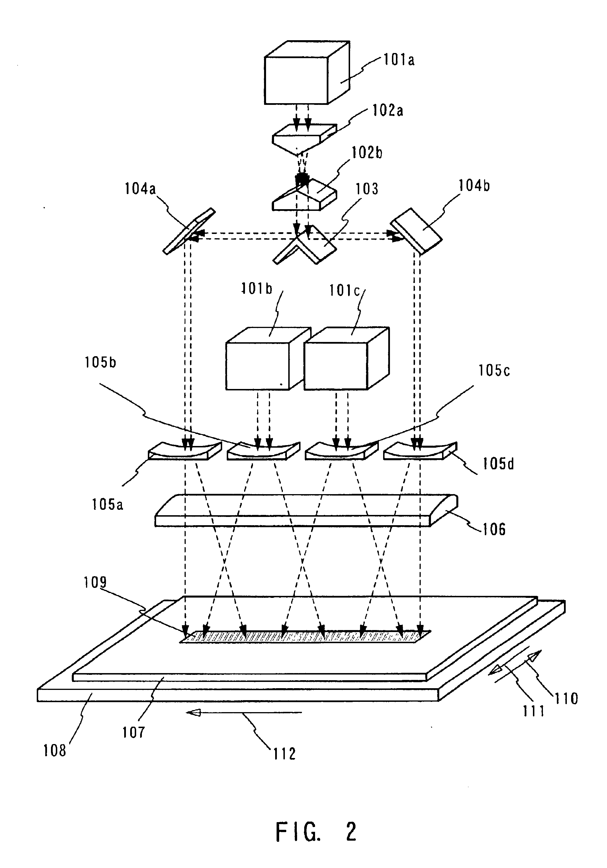
This embodiment describes an example of laser irradiation apparatus for carrying out the present invention with reference to FIG. 3.

Laser beams emitted from lasers 101b and 101c are widened in the longitudinal direction by concave cylindrical lenses 105b and 105c, respectively. Though not shown in the drawing, beam collimators for changing the laser beams emitted from the lasers 101b and 101c into parallel beams and beam expanders for expanding laser light may be placed between the lasers 101b and 101c and the concave cylindrical lenses 105b and 105c. The laser beams reach a substrate 107 after they are collected in the lateral direction by a convex cylindrical lens 106 that has curvature in the lateral direction.

On the other hand, laser light emitted from a laser 101a is divided by a mirror 103 in two directions. Though not shown in the drawing, a beam collimator for changing a laser beam emitted from the laser 101a into parallel beams and a beam expander for expanding laser light ...

embodiment 3

This embodiment describes with reference to FIG. 4 apparatus and method for irradiating a substrate with laser light from lasers placed on both sides of the substrate.

Lasers 101a to 101c are arranged such that they are staggered with respect to a substrate 107. Laser beams emitted from the lasers 101a to 101c are collected in the lateral direction by convex cylindrical lenses 122a to 122c, respectively, and then reach the substrate 107. Though not shown in the drawing, beam collimators for changing the laser beams emitted from the lasers 101a to 101c into parallel beams and beam expanders for expanding laser light may be placed between the lasers 101a to 101c and the convex cylindrical lenses 122a to 122c.

On the other hand, laser light emitted from a laser 101d is divided by mirrors 123a and 123b in two directions. This is for forming, on the substrate 107, laser light 129 every part of which has enough energy density. By dividing the laser light emitted from the laser 101d (initia...


PUM

PropertyMeasurementUnit
wavelengthaaaaaaaaaa
aspect ratioaaaaaaaaaa

Abstract

At edges of laser light on an irradiation surface or in the vicinity thereof, the energy density is attenuated gradually due to aberration of a lens or the like. Since such regions (attenuation regions) do not have enough energy density for annealing of an irradiation object, uniform annealing of the irradiation object is not possible.
In the present invention, one of the plural laser beams is divided into two laser beams so that each section of the two laser beams serves as an edge of the resultant laser light. Each attenuation region of the two laser beams is synthesized with an attenuation region of another laser beam. In this way, laser light every part of which has an energy density suitable for satisfactory annealing of an irradiation object can be obtained from plural laser beams having attenuation regions.

Description

BACKGROUND OF THE INVENTION1. Field of the InventionThe present invention relates to a method of annealing a semiconductor film using a laser light (hereinafter referred to as laser annealing) and to a laser irradiation apparatus for conducting the method (apparatus including a laser and an optical system for guiding a laser light emitted from the laser to an object to be processed). Also, the present invention relates to a method of manufacturing a semiconductor device including said step of laser annealing. Note that the term semiconductor device mentioned here indicates semiconductor devices in general which can function by utilizing semiconductor characteristics, and includes electro-optical devices such as a liquid crystal display device, a light emitting device and an electronic device including the electro-optical device as a component.2. Description of the Related ArtIn recent years, there has been widely studied a technique of conducting laser annealing to a semiconductor f...

Claims


Application Information

Patent Timeline
Patent Type & Authority Patents(United States)
IPC IPC(8): B23K26/067B23K26/073B23K26/06H01L21/02H01L21/20H01L21/268H01S3/10H01L21/336H01L29/786
CPCB23K26/0604B23K26/0608B23K26/067B23K26/0732H01L21/268B23K26/0738H01L21/2026B23K26/0736B23K2201/40B23K2101/40H01L21/02683H01L21/02502H01L21/02488H01L21/02422H01L21/02529H01L21/0242H01L21/02672H01L21/02425H01L21/02686H01L21/02678H01L21/02532H01L21/02381H01L21/02691H01S3/10
Inventor TANAKA, KOICHIRO
Owner SEMICON ENERGY LAB CO LTD
Why Eureka
Try Eureka