Ferroelectric capacitor, process for production thereof and semiconductor device using the same

a ferroelectric capacitor and capacitor technology, applied in the direction of instruments, scanning probe techniques, vacuum evaporation coating, etc., can solve the problems of ferroelectric capacitors not having sufficient fatigue properties, ferroelectric capacitors with polarization fatigue, etc., to reduce fatigue and efficiently produce ferroelectric capacitors

Inactive Publication Date: 2005-02-15
FUJITSU LTD
View PDF9 Cites 23 Cited by
  • Summary
  • Abstract
  • Description
  • Claims
  • Application Information

AI Technical Summary

Benefits of technology

Under these circumstances, an object of the present invention is to provide a ferroelectric capacitor which shows reduced fatigue and is suitable as a large-capacity nonvolatile memory, a process for efficiently producing the ferroelectric capacitor, and a high-performance semiconductor device having the ferroelectric capacitor.

Problems solved by technology

However, when the ferroelectric capacitor having the thus-formed ferroelectric is applied to a nonvolatile memory and the ferroelectric undergoes repetitive switching process (repetitive polarization reversal), it induces “fatigue (polarization fatigue)” in which the polarization of the ferroelectric decreases.
Another attempt has been made to form a ferroelectric capacitor having an IrO2 / PZT / Ir multilayer structure by MOCVD, but the resulting ferroelectric capacitor does not have sufficiently improved fatigue properties.

Method used


Image

  • Ferroelectric capacitor, process for production thereof and semiconductor device using the same
  • Ferroelectric capacitor, process for production thereof and semiconductor device using the same
  • Ferroelectric capacitor, process for production thereof and semiconductor device using the same

Examples


example 1

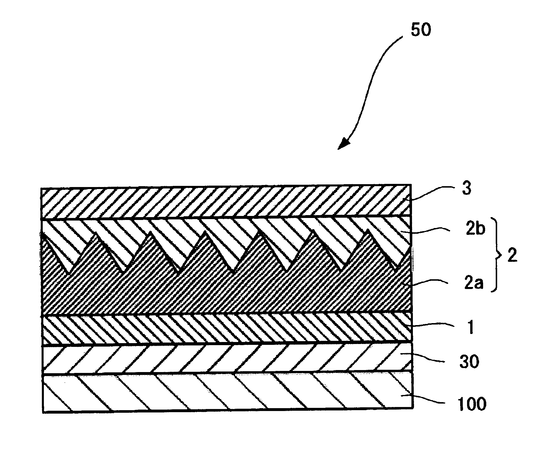
A ferroelectric capacitor 50 shown in FIG. 1 was produced in the following manner.

Initially, a lower electrode 1 was formed by sputtering to a thickness of about 150 nm on a SiO2 film 30 on a silicon substrate 100.

A Pb(Zr,Ti)O3 [PZT] film 2a was formed by MOCVD on the lower electrode 1. More specifically, the Pb(Zr,Ti)O3 [PZT] film was formed at a temperature of 620° C. feeding Pb(DPM)2 as a Pb source at 0.37 ml / min., Zr(dmhd)4 as a Zr source at 0.31 ml / min., and Ti(O-iPr)2(DPM)2 as a Ti source at 0.21 ml / min. at an oxygen partial pressure of 5 Torr (666 Pa). Each of these materials was dissolved in tetrahydrofuran (THF) in a concentration of 3% by mole to yield a solution, and the solution was conveyed to a vaporizer. The solution containing THF and the material was vaporized at 260° C. in the vaporizer, was mixed with oxygen gas to form a source gas, and the source gas was sprayed to the lower electrode using a showerhead. The film-forming time of the Pb(Zr,Ti)O3 [PZT] film 2a was...

example 2

Production of Semiconductor Device

The semiconductor device was produced in the following manner.

Initially, as shown in FIG. 4, an element-separation dielectric film was formed by local oxidation of silicon (LOCOS) on a surface of a silicon Si substrate 100 to define and separate an element region. The element-separation dielectric film can be formed by LOCOS or by forming grooves on the silicon substrate and embedding a dielectric film in the grooves. The silicon substrate 100 may be of either n-type or p-type.

A transistor having a side-wall dielectric film with a gate electrode 18 and a source-drain doped layer was formed in the element region. An interlayer dielectric film 22 composed of a silicone oxide was entirely formed by CVD, followed by smoothing the surface of the interlayer dielectric film 22 by chemical-mechanical polishing (CMP).

Next, contact holes reaching the source-drain doped layer were formed in the interlayer dielectric film 22 by photolithography, and a Ti film a...


PUM

PropertyMeasurementUnit
surface roughnessaaaaaaaaaa
temperatureaaaaaaaaaa

Abstract

A ferroelectric capacitor includes a pair of electrodes, and at least one ferroelectric held between the pair of electrodes, in which the ferroelectric includes a first ferroelectric layer having a surface roughness (RMS) determined with an atomic force microscope of 10 nm or more; and a second ferroelectric layer being arranged adjacent to the first ferroelectric layer and having an RMS of 5 nm or less. A process produces such a ferroelectric capacitor by forming a first ferroelectric layer on or above one of a pair of electrodes at a temperature equal to or higher than a crystallization temperature at which the first ferroelectric layer takes on a ferroelectric crystalline structure, and forming a second ferroelectric layer on the first ferroelectric layer at a temperature lower than a crystallization temperature at which the second ferroelectric layer takes on a ferroelectric crystalline structure.

Description

CROSS-REFERENCE TO RELATED APPLICATIONSThis application is based upon and claims the benefits of the priority from the prior Japanese Patent Application No. 2003-002577, filed in Jan. 8, 2003, the entire contents of which are incorporated herein by reference.BACKGROUND OF THE INVENTION1. Field of the InventionThe present invention relates to a ferroelectric capacitor which shows less fatigue and is suitable as a large-capacity nonvolatile memory, a process for efficiently producing the ferroelectric capacitor, and a high-performance semiconductor device having the ferroelectric capacitor.2. Description of the Related ArtFerroelectrics have excellent ferroelectricity, piezoelectricity and pyroelectricity and are widely used in, for example, a variety of memories, actuators, and sensors. For example, such ferroelectrics have been applied to nonvolatile memories by utilizing the hysteresis of the ferroelectrics. Certain ferroelectric capacitors comprising a lower electrode, a ferroelec...

Claims


Application Information

Patent Timeline
Patent Type & Authority Patents(United States)
IPC IPC(8): H01L21/70H01L21/02H01L27/115H01L21/8246C23C14/08C23C16/40G01Q30/04G01Q30/10G01Q70/04G01Q70/14H01L21/316H01L27/105
CPCH01L27/11502H01L28/56H01L27/11507H10B53/30H10B53/00
Inventor MATSUURA, OSAMUMARUYAMA, KENJITAKAI, KAZUAKI
Owner FUJITSU LTD
Why Eureka
Try Eureka