Structure and method for fabricating configurable transistor devices utilizing the formation of a compliant substrate for materials used to form the same

a transistor device and substrate technology, applied in the direction of semiconductor laser structure details, semiconductor lasers, lasers, etc., can solve the problems of low crystalline quality of monocrystalline materials, and it has been difficult if not impossible to integrate these materials into a common monolithic devi

Inactive Publication Date: 2005-02-15
NXP USA INC
View PDF748 Cites 31 Cited by
  • Summary
  • Abstract
  • Description
  • Claims
  • Application Information

AI Technical Summary

Problems solved by technology

These attempts have generally been unsuccessful because lattice mismatches between the host crystal and the grown crystal have caused the resulting layer of monocrystalline material to be of low crystalline quality.
However, it has heretofore been difficult if not impossible to integrated these materials in a common monolithic device.

Method used


Image

  • Structure and method for fabricating configurable transistor devices utilizing the formation of a compliant substrate for materials used to form the same
  • Structure and method for fabricating configurable transistor devices utilizing the formation of a compliant substrate for materials used to form the same
  • Structure and method for fabricating configurable transistor devices utilizing the formation of a compliant substrate for materials used to form the same

Examples


example 2

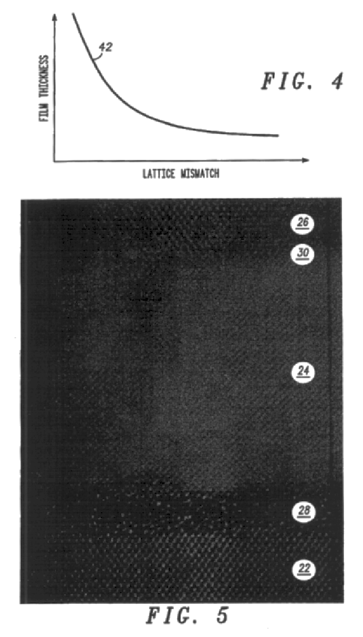
In accordance with a further embodiment of the invention, monocrystalline substrate 22 is a silicon substrate as described above. The accommodating buffer layer is a monocrystalline oxide of strontium or barium zirconate or hafnate in a cubic or orthorhombic phase with an amorphous intermediate layer of silicon oxide formed at the interface between the silicon substrate and the accommodating buffer layer. The accommodating buffer layer can have a thickness of about 2-100 nm and preferably has a thickness of at least 5 nm to ensure adequate crystalline and surface quality and is formed of a monocrystalline SrZrO3, BaZrO3, SrHfO3, BaSnO3 or BaHfO3. For example, a monocrystalline oxide layer of BaZrO3 can grow at a temperature of about 700 degrees C. The lattice structure of the resulting crystalline oxide exhibits a 45 degree rotation with respect to the substrate silicon lattice structure.

An accommodating buffer layer formed of these zirconate or hafnate materials is suitable for the...

example 3

In accordance with a further embodiment of the invention, a structure is provided that is suitable for the growth of an epitaxial film of a monocrystalline material comprising a II-VI material overlying a silicon substrate. The substrate is preferably a silicon wafer as described above. A suitable accommodating buffer layer material is SrxBa1−xTiO3, where x ranges from 0 to 1, having a thickness of about 2-100 nm and preferably a thickness of about 5-15 nm. Where the monocrystalline layer comprises a compound semiconductor material, the II-VI compound semiconductor material can be, for example, zinc selenide (ZnSe) or zinc sulfur selenide (ZnSSe). A suitable template for this material system includes 1-10 monolayers of zinc-oxygen (Zn—O) followed by 1-2 monolayers of an excess of zinc followed by the selenidation of zinc on the surface. Alternatively, a template can be, for example, 1-10 monolayers of strontium-sulfur (Sr—S) followed by the ZnSeS.

example 4

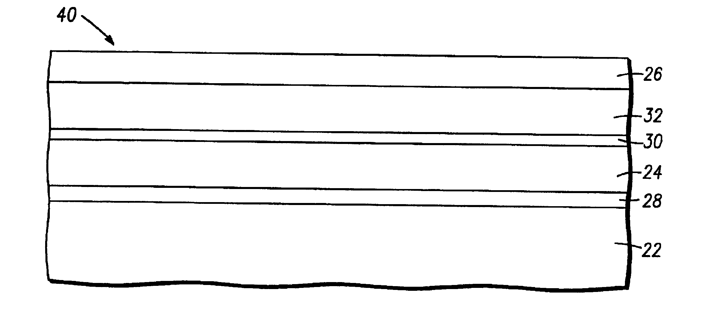
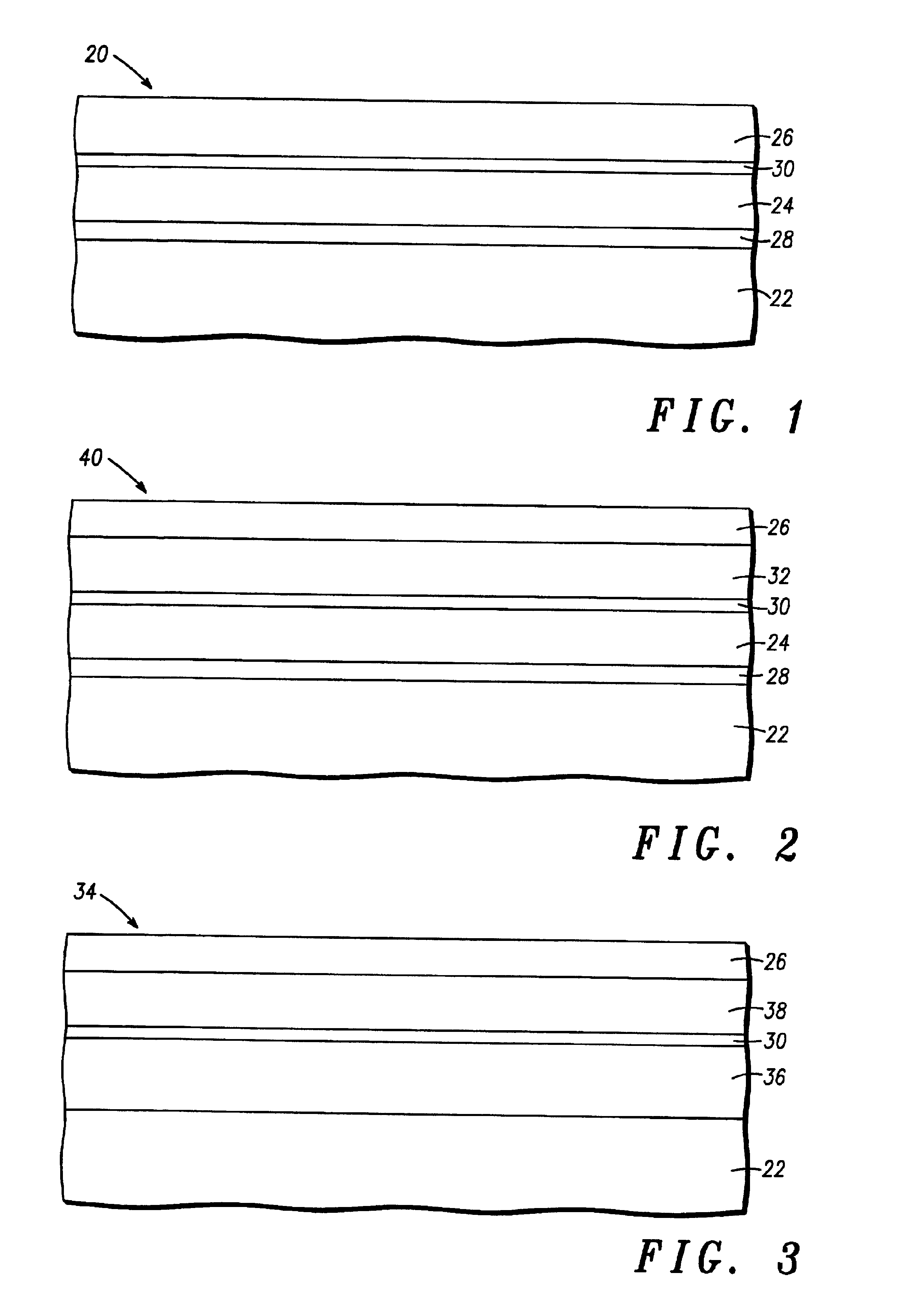
This embodiment of the invention is an example of structure 40 illustrated in FIG. 2. Substrate 22, accommodating buffer layer 24, and monocrystalline material layer 26 can be similar to those described in example 1. In addition, an additional buffer layer 32 serves to alleviate any strains that might result from a mismatch of the crystal lattice of the accommodating buffer layer and the lattice of the monocrystalline material. Buffer layer 32 can be a layer of germanium or a GaAs, an aluminum gallium arsenide (AlGaAs), an indium gallium phosphide (InGaP), an aluminum gallium phosphide (AlGaP), an indium gallium arsenide (InGaAs), an aluminum,indium phosphide (AlInP), a gallium arsenide phosphide (GaAsP), or an indium gallium phosphide (InGaP) strain compensated superlattice. In accordance with one aspect of this embodiment, buffer layer 32 includes a GaAsxP1−x superlattice, wherein the value of x ranges from 0 to 1. In accordance with another aspect, buffer layer 32 includes an Iny...


PUM

PropertyMeasurementUnit
thicknessaaaaaaaaaa
diameteraaaaaaaaaa
thicknessaaaaaaaaaa

Abstract

A semiconductor structure includes a monocrystalline silicon substrate, an amorphous oxide material overlying the monocrystalline silicon substrate, a monocrystalline perovskite oxide material overlying the amorphous oxide material, and a monocrystalline compound semiconductor material overlying the monocrystalline perovskite oxide material. A composite transistor includes a first transistor having first active regions formed in the monocrystalline silicon substrate, a second transistor having second active regions formed in the monocrystalline compound semiconductor material, and a mode control terminal for controlling the first transistor and the second transistor.

Description

FIELD OF THE INVENTIONThis invention relates generally to semiconductor structures and devices and to a method for their fabrication. More particularly, this invention relates to semiconductor structures and devices and to the fabrication and use of semiconductor structures, devices and integrated circuits that include a monocrystalline material layer comprised of semiconductor material, compound semiconductor material and / or other types of material such as metals and non-metals.BACKGROUND OF THE INVENTIONSemiconductor devices often include multiple layers of conductive, insulating and semiconductive layers. Often, the desirable properties of such layers improve with the crystallinity of the layer. For example, the electron mobility and band gap of semiconductive layers improves as the crystallinity of the layer increases. Similarly, the free electron concentration of conductive layers and the electron charge displacement and electron energy recoverability of insulative or dielectri...

Claims


Application Information

Patent Timeline
Patent Type & Authority Patents(United States)
IPC IPC(8): H01L21/70H01L21/02H01L21/338H01L21/8258H01L27/06H01L21/20H01L27/15H01S5/00H01S5/02H01S5/026
CPCH01L27/0605H01L29/66848H01L21/8258H01L21/02381H01L21/02488H01L21/02505H01L21/02513H01L21/02521H01S2301/173H01L27/15H01S5/021H01S5/0261
Inventor EMRICK, RUDY M.BOSCO, BRUCE ALLENHOLMES, JOHN E.FRANSON, STEVEN JAMESROCKWELL, STEPHEN KENT
Owner NXP USA INC
Why Eureka
Try Eureka