Low-voltage punch-through bi-directional transient-voltage suppression devices having surface breakdown protection and methods of making the same

Inactive Publication Date: 2005-02-22
GEN SEMICON
View PDF7 Cites 4 Cited by
  • Summary
  • Abstract
  • Description
  • Claims
  • Application Information

AI Technical Summary

Benefits of technology

One advantage of the present invention is that a low-voltage bi-directional transient-voltage suppressor is provided that has a low leakage current.
A further advantage of the present invention is that a low-voltage bi-directional transient-voltage suppressor is provided that has a lower capacitance than the Zener transient-voltage suppression device with the same breakdown voltage.
Yet another advantage of the present invention is that a low-voltage bi-directional transient-voltage suppressor is provided which has symmetric current-voltage characteristics. This is in contrast to, for example, the n+p−p+n+ devices described in U.S. Pat. No. 5,880,511.
Yet another advantage of the present invention is that a low-voltage bi-directional transient-voltage suppressor is provided which has acceptable clamping characteristics at high currents. More specifically, as noted above, U.S. Pat. No. 5,880,511 claims that n+pn+ uniform-base punch-through devices suffer from poor clamping characteristics at high currents. A base with a uniform carrier concentration is indeed in danger of becoming intrinsic at temperatures that are lower than most other constructions. High temperature protection is important, for example, during power surges in which the region bordering the junction can rise by several hundred ° C. within milliseconds. A base with a high-doped portion and a low-doped portion will perform better than a uniformly doped base of intermediate doping co

Problems solved by technology

Such damage can arise from overvoltage conditions caused by electrostatic discharge, inductively coupled spikes, or other transient conditions.
These devices perform well at higher voltages, but run into problems, specifically large leakage currents and high capacitance, at low

Method used


Image

  • Low-voltage punch-through bi-directional transient-voltage suppression devices having surface breakdown protection and methods of making the same
  • Low-voltage punch-through bi-directional transient-voltage suppression devices having surface breakdown protection and methods of making the same
  • Low-voltage punch-through bi-directional transient-voltage suppression devices having surface breakdown protection and methods of making the same

Examples


Example

EXAMPLE

Six wafers were made in a trial run according to the procedures to follow.

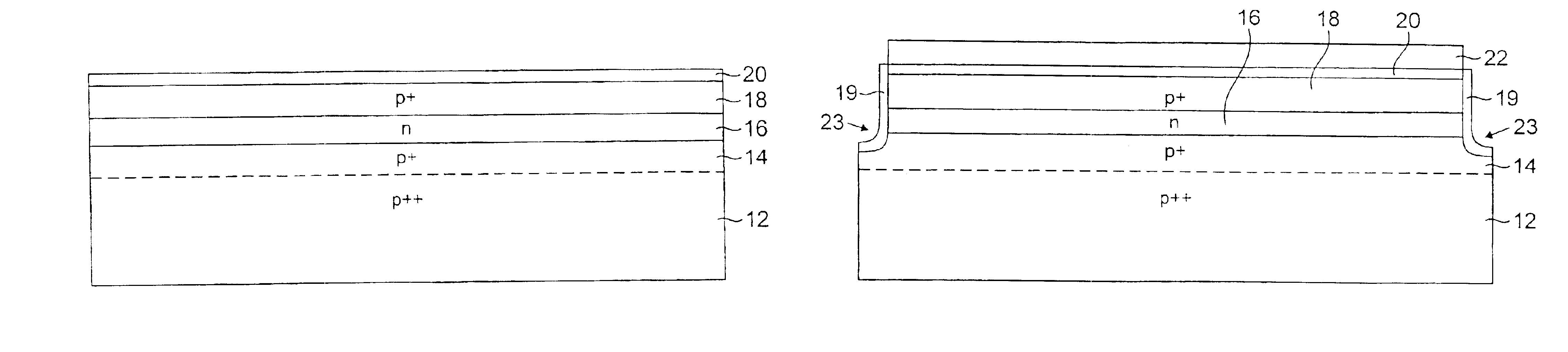
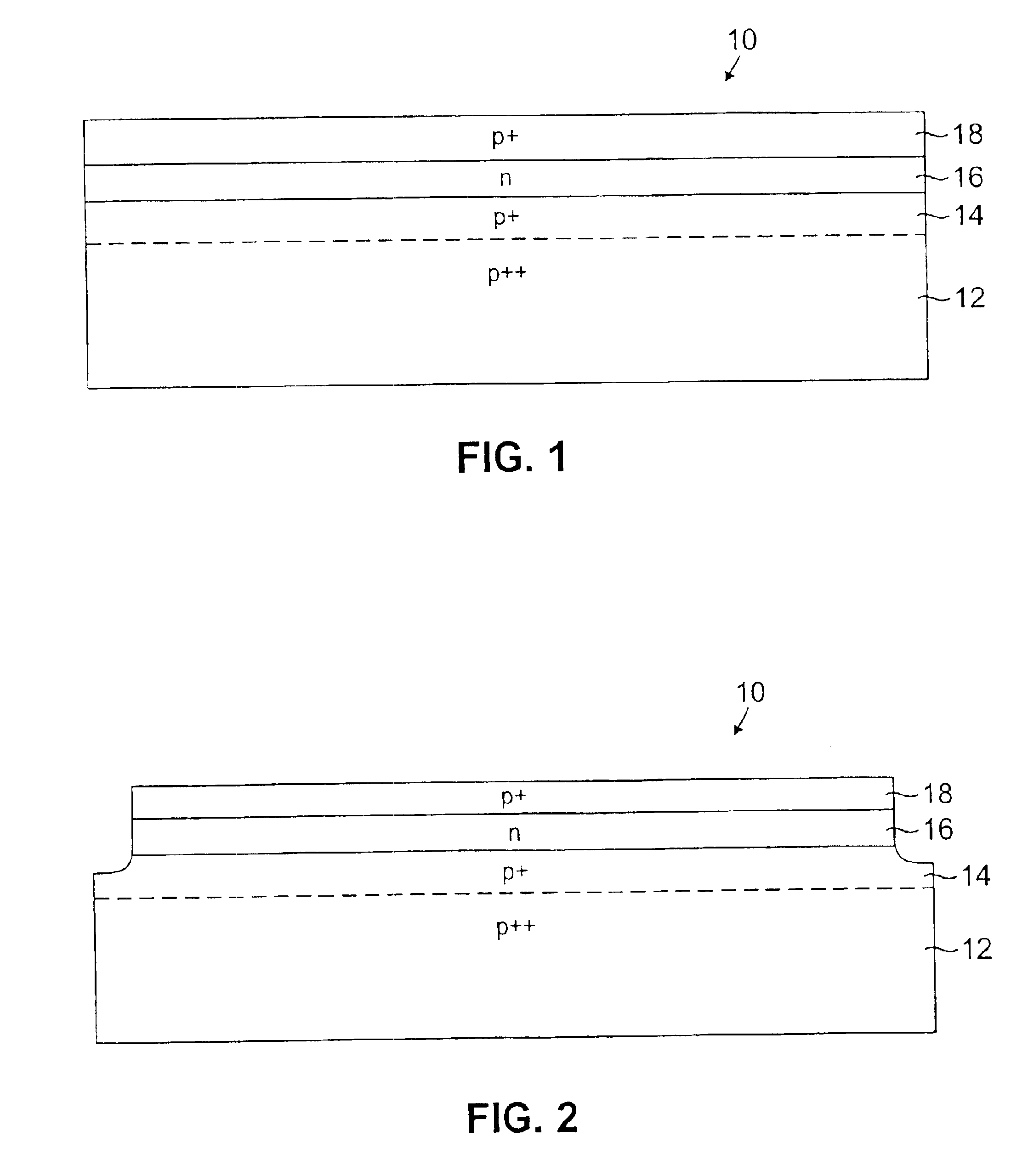
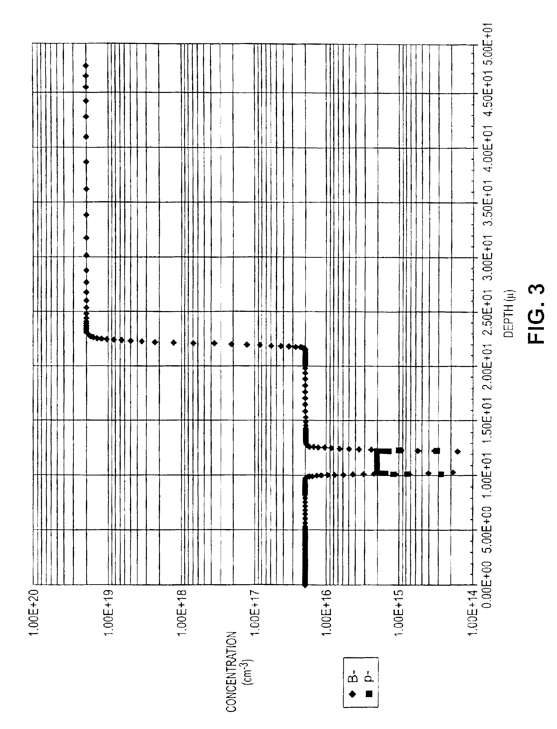
Three epitaxial layers were grown in one continuous process step. The wafers were not exposed to air and not cooled down during the continuous growth of the three layers. The p++ substrates had resistivities ranging from 0.005 to 0.002 ohm-cm. The first p+ epitaxial layer was 10 microns in thickness and had a resistivity of 0.5 ohm-cm. The n epitaxial layer was 2.5 microns in thickness and had a resistivity of 2.5 ohm-cm. The second p+ epitaxial layer had a thickness of 20 micron and a resistivity of 0.5 ohm-cm. After epitaxial layer growth, a boron deposition step was performed for 1 hour at 1100° C., with a slow temperature ramp up and ramp down. This deposition is performed on both sides of the wafer in a single step, creating ohmic contacts (p++ regions).

A silicon nitride layer having a thickness of 200 nm was then deposited using conventional techniques.

A patterned photoresist layer was then applie...


PUM


Abstract

A method of making a bi-directional transient voltage suppression device is provided, which comprises: (a) providing a p-type semiconductor substrate; (b) epitaxially depositing a lower semiconductor layer of p-type conductivity; (c) epitaxially depositing a middle semiconductor layer of n-type conductivity over the lower layer; (d) epitaxially depositing an upper semiconductor layer of p-type conductivity over the middle layer; (e) heating the substrate, the lower epitaxial layer, the middle epitaxial layer and the upper epitaxial layer; (f) etching a mesa trench that extends through the upper layer, through the middle layer and through at least a portion of the lower layer, such that the mesa trench defines an active area for the device; and (g) thermally growing an oxide layer on at least those portions of the walls of the mesa trench that correspond to the upper and lower junctions of the device.

Description

FIELD OF THE INVENTIONThe present invention relates to semiconductor devices. More particularly, the present invention relates to low-voltage punch-through bi-directional transient-voltage suppression devices having significant protection against surface breakdown.BACKGROUND OF THE INVENTIONElectronic circuits that are designed to operate at low supply voltages are common in the electronics industry. Current trends toward a reduction in circuit operating voltage dictate a corresponding reduction in the maximum voltage that the circuitry can withstand without incurring damage. Such damage can arise from overvoltage conditions caused by electrostatic discharge, inductively coupled spikes, or other transient conditions. Hence, demand presently exists for transient-voltage suppressors having low breakdown voltages, for example, voltages in the 3-6 volt range.One traditional device for overvoltage protection is the reversed biased p+n+ Zener diode. These devices perform well at higher vo...

Claims


Application Information

Patent Timeline
IPC IPC(8): H01L21/02H01L29/66H01L21/329H01L29/861H01L27/02
CPCH01L27/0259H01L29/0607H01L29/8618H01L29/66121Y10S438/912Y10S438/965H01L21/20
Inventor EINTHOVEN, WILLEM G.GINTY, ANTHONYWALSH, AIDAN
Owner GEN SEMICON
Why Eureka
Try Eureka