

ESD protection devices and methods to reduce trigger voltage
a protection device and trigger voltage technology, applied in semiconductor devices, semiconductor/solid-state device details, transistors, etc., can solve the problems of increasing the risk of external environment impact, local heating, and eventually damaging the nmos, and achieve the effect of reducing the breakdown voltag
- Summary
- Abstract
- Description
- Claims
- Application Information
AI Technical Summary
Benefits of technology
Problems solved by technology
Method used
Image

Examples
Embodiment Construction
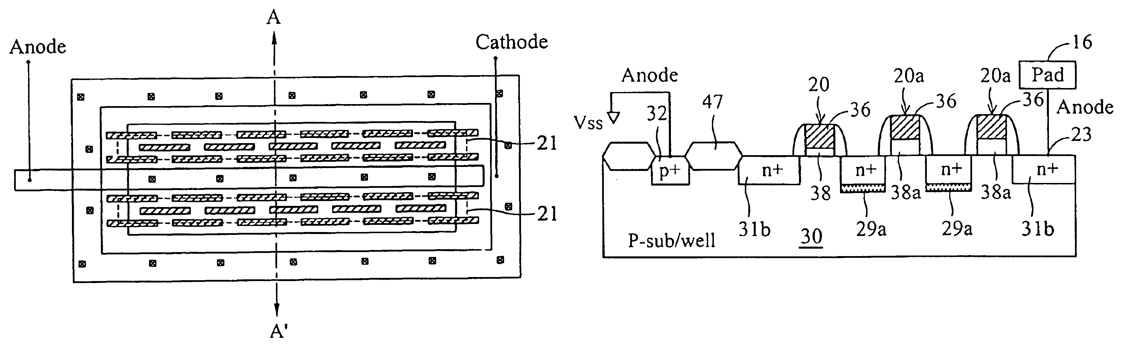
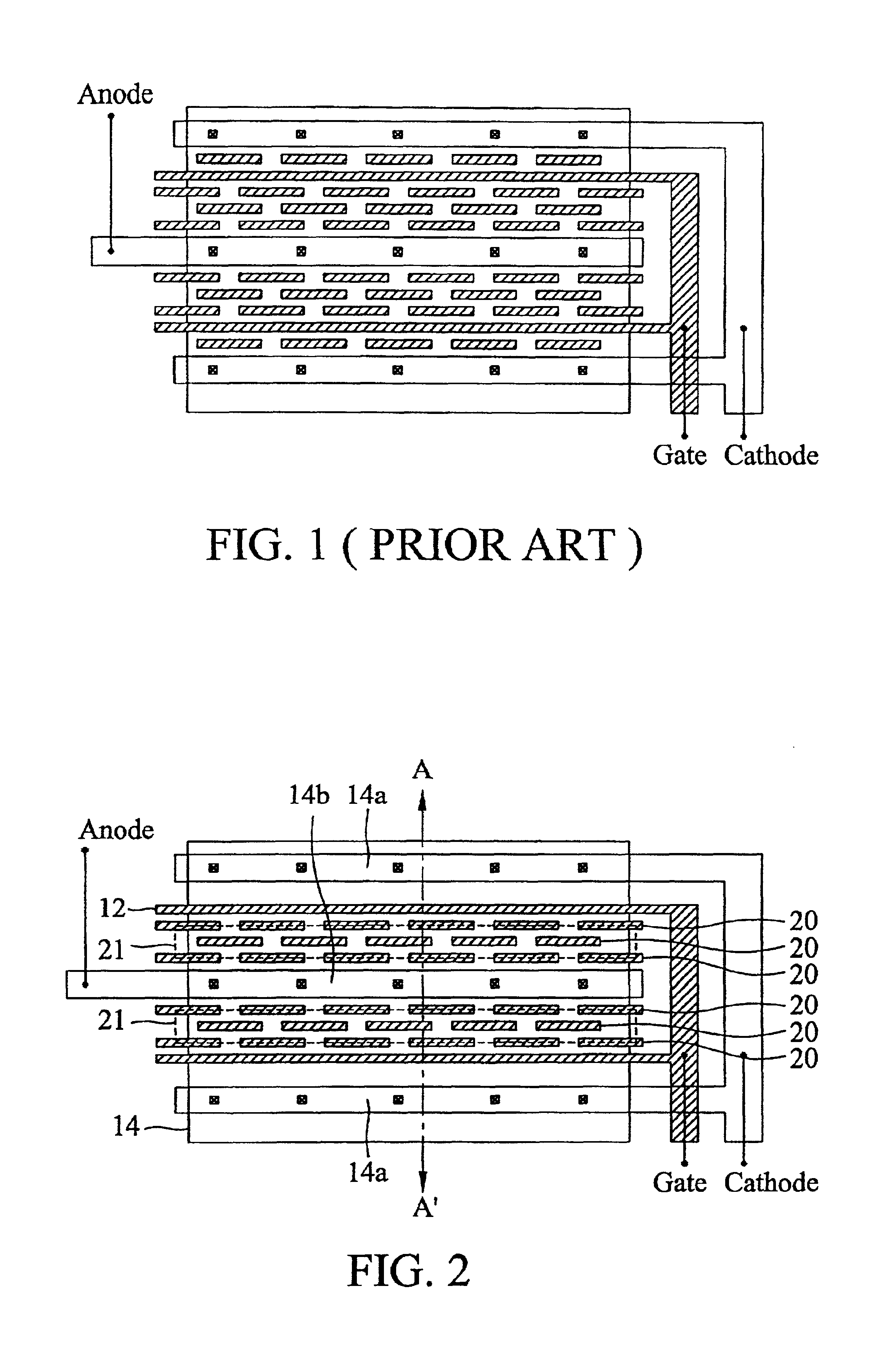
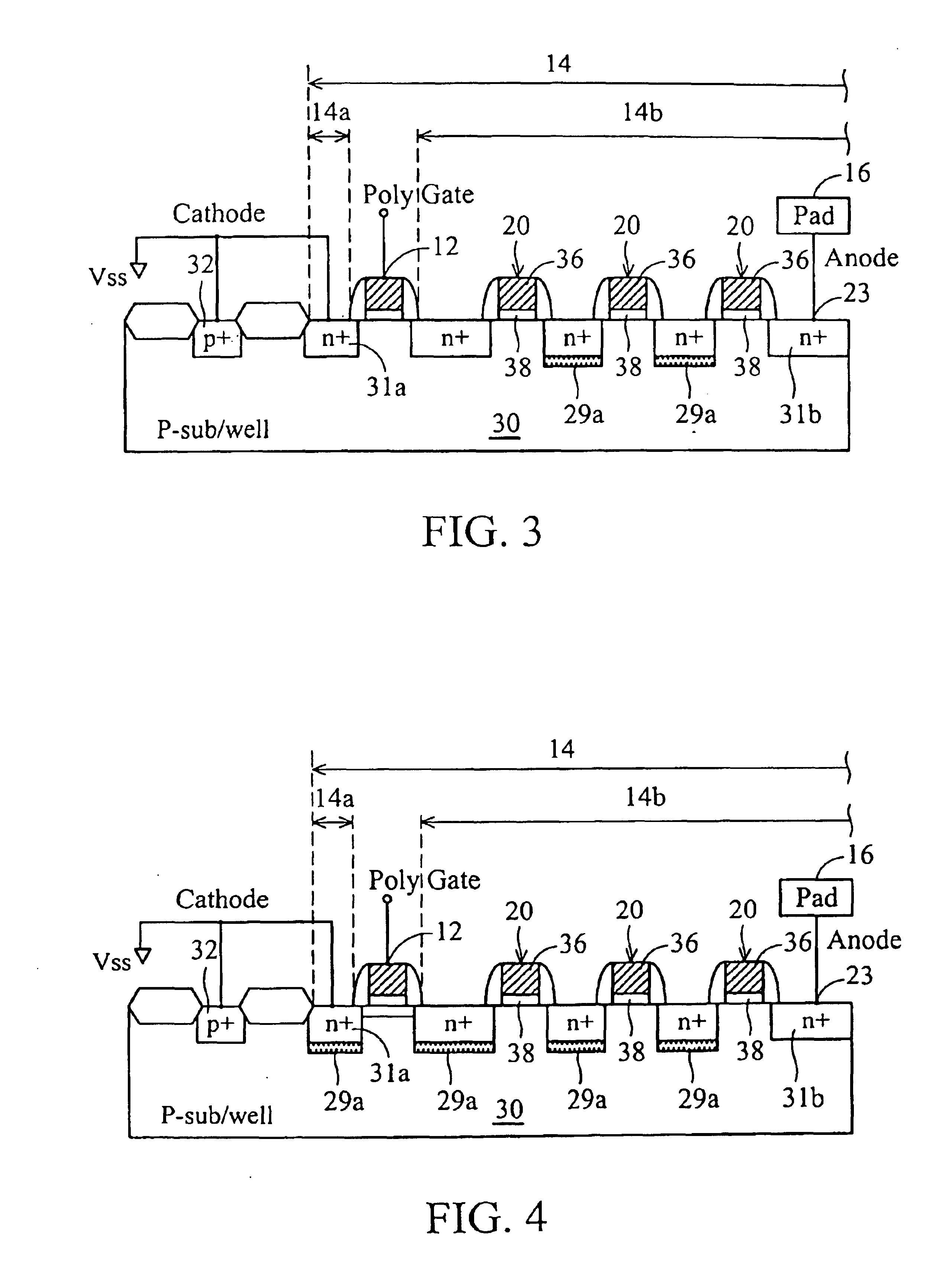
FIG. 2 shows a layout view of an NMOS structure according to the present invention. FIG. 3 is a cross-section of the NMOS structure in FIG. 2 along a portion of line A-A′.
The ESD protection device in FIG. 2 is a multi-finger-type NMOS with two poly gates 12 coupled together. An active region 14 is surrounded by a field oxide (FOX) isolation region, which is typically formed by local oxidation (LOCOS) or shallow trench isolation (STI). The active region 14 is typically ion-implanted by negative-type ions and then annealed by thermal cycles to form heavily n-doped (n+) layers. The ion implant is blocked by any poly gate, poly segment or field oxide region present within the active region. Within the active region 14, two channel regions under the poly gates 12 are formed. The portion of the active region 14 between the two poly gates 12 is referred to as a drain diffusion region 14b, serving as an anode and coupled to a pad 16, and the portions of the active region 14 sandwiching the ...
PUM
 Abstract
Description
Claims
Application Information