Semiconductor light emitting element and method for fabricating the same

a technology of semiconductor light emitting elements and semiconductor materials, which is applied in the direction of semiconductor lasers, natural mineral layered products, transportation and packaging, etc., can solve the problem of not knowing whether the characteristics of gan materials are durable enough for practical use, and achieve the effects of low threshold current, simple structure and high performan

Inactive Publication Date: 2005-03-01
PANASONIC CORP
View PDF14 Cites 18 Cited by
  • Summary
  • Abstract
  • Description
  • Claims
  • Application Information

AI Technical Summary

Benefits of technology

Alternatively, the method for fabricating a semiconductor light emitting element of this invention includes the steps of: forming a first cladding layer on a substrate; forming a second cladding layer on the first cladding layer; forming an active layer on the second cladding layer; forming a third cladding layer on the active layer; forming an insulating film on faces of the substrate, the first cladding layer, the second cladding layer, the active layer, and the third cladding layer vertical to a depositing direction; removing a portion of the insulating film so as to expose the side face of the first cladding layer; and etching so that the first cladding layer can be etched faster than the insulating film.
Thus, the invention described herein makes possible the advantages of (1) providing a semiconductor light emitting element with high performance and a simple structure where the strain characteristic of an electronic band structure unique to a hexagonal-system compound semiconductor is utilized, i.e., providing a semiconductor light emitting element with a low threshold current by applying anisotropic strain to the c plane of a hexagonal-system compound semiconductor, and (2) providing a method for fabricating such a semiconductor light emitting element.

Problems solved by technology

Therefore, it is uncertain whether GaN material can provide characteristics durable enough for practical use when it is used as an element having a structure similar to that used for conventional cubic-system materials.

Method used


Image

  • Semiconductor light emitting element and method for fabricating the same
  • Semiconductor light emitting element and method for fabricating the same
  • Semiconductor light emitting element and method for fabricating the same

Examples


example 1

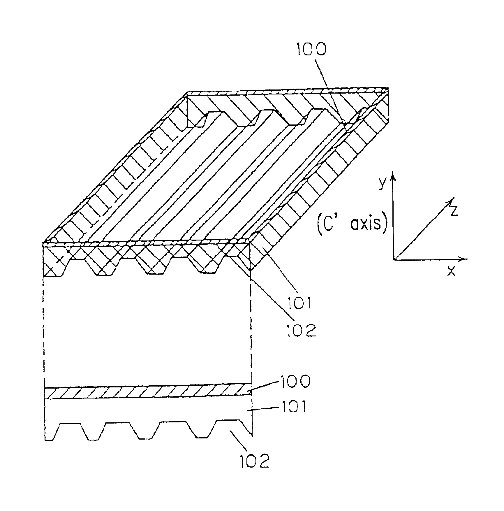
The semiconductor light emitting element of Example 1 according to the present invention will be described with reference to FIG. 4. An AlGaInN material which is a III-V group compound semiconductor is used as a hexagonal-system compound semiconductor. Strain is applied in a direction parallel to the c plane. When a wurtzite-type material is used for an AlGaInN light emitting layer 100, the band structure (valence band) can be changed by applying uniaxial strain in a direction vertical to the (0001) axis (parallel to the c plane). As a result, the characteristics of the light emitting element improve as described above.

By forming stripe-shaped grooves 102 on a sapphire substrate 101 as shown in FIG. 4, the directivity of the thermal expansion coefficient is exhibited on the substrate 101. By this formation of the grooves 102, it is possible to apply uniaxial strain in the x direction shown in FIG. 4 to the AlGaInN light emitting layer 100 grown on the surface of the substrate 101 op...

example 2

FIG. 10 is a sectional view of a wurtzite-type InxGa1-xN / AlyGa1-yN quantum well semiconductor laser of Example 2 according to the present invention. InxGa1-xN and AlyGa1-yN are used for a quantum well layer and a barrier layer, respectively.

Referring to FIG. 10, an AlN buffer layer 202, an n-AlzGa1-zN cladding layer 203, an AlyGa1-yN first optical guide layer 204, an InxGa1-xN / GaN multiple quantum well active layer 205 (a multilayer structure of InxGa1-xN quantum well layers and GaN quantum well layers), an AlyGa1-yN second optical guide layer 206, and a p-AlzGa1-zN cladding layer 207 are consecutively formed in this order on a (1100) LiTaO3 substrate 201 by MOVPE.

A ridge stripe 208 is formed by etching, and an SiO2 insulating film 209 is formed over the top surface of the resultant structure. Openings 210 and 211 are formed at the SiO2 insulating film 209 for current injection. Finally, an anode electrode 212 and a cathode electrode 213 are formed.

The layers constituting the wurtzi...

example 3

FIG. 13 is a sectional view of a wurtzite-type InGaN / AlGaN quantum well semiconductor laser of Example 3 according to the present invention.

Referring to FIG. 13, an AlN buffer layer 302, an n-AlzGa1-zN cladding layer 303, an AlyGa1-yN first optical guide layer 304, an InxGa1-xN / GaN multiple quantum well active layer 305, an AlyGa1-yN second optical guide layer 306, a p-AlzGa1-zN first cladding layer 307, and a p-Alz′Ga1-z′N strain generating layer 308 are consecutively formed in this order on a (0001) sapphire substrate 301 by crystal growth. Then, the resultant structure is taken out from a crystal growth apparatus, and the p-Alz′Ga1-z′N strain generating layer 308 is shaped into a stripe with a width of 2 mm by etching. The resultant structure is placed in the crystal growth apparatus again, and a p-AlzGa1-zN second cladding layer 309 is formed. An SiO2 insulating film 310 is then formed over the top surface of the resultant structure. Openings 311 and 312 are formed at the SiO2 i...


PUM

PropertyMeasurementUnit
widthaaaaaaaaaa
widthaaaaaaaaaa
temperatureaaaaaaaaaa

Abstract

The semiconductor laser of this invention includes an active layer formed in a c-axis direction, wherein the active layer is made of a hexagonal-system compound semiconductor, and anisotropic strain is generated in a c plane of the active layer.

Description

BACKGROUND OF THE INVENTION1. Field of the InventionThe present invention relates to a short-wavelength semiconductor light emitting element used in the fields of optical communications, optical information processing, and the like, and a method for fabricating the same.2. Description of the Related ArtIn recent years, with increased demands for short-wavelength semiconductor light emitting elements in various fields, studies focusing mainly on ZnSe and GaN as the materials for such elements have been vigorously conducted. As for ZnSe material, a short-wavelength semiconductor laser with an oscillation wavelength of about 500 nm has succeeded in oscillating consecutively at room temperature. Now, study and development for practical use of this material is under way. As for GaN material, a blue light emitting diode with high luminance has recently been realized. The reliability of this material as the light emitting diode is by no means inferior to that of other materials for semicon...

Claims


Application Information

Patent Timeline
Patent Type & Authority Patents(United States)
IPC IPC(8): H01S5/32H01S5/00H01S5/323H01S5/223H01S5/20H01S5/02H01L33/16H01L33/32
CPCB82Y20/00H01S5/2201H01S5/34333Y10T428/12528H01L33/32H01S5/0207H01S5/0213H01S5/02272H01S5/2068H01S5/2232H01S5/2237H01S5/24H01S5/3201H01S5/3202H01S5/3203H01S5/32308H01S5/32341H01S5/3403H01S2301/173H01S2304/04H01S2304/12Y10S257/918H01L33/16H01S5/320225H01S5/0237
Inventor KAMIYAMA, SATOSHISUZUKI, MASAKATSUUENOYAMA, TAKESHIOHNAKA, KIYOSHITAKAMORI, AKIRAMANNOH, MASAYAKIDOGUCHI, ISAOADACHI, HIDETOISHIBASHI, AKIHIKOFUKUHISA, TOSHIYAKUMABUCHI, YASUHITO
Owner PANASONIC CORP
Why Eureka
Try Eureka