Hybrid bulk/silicon-on-insulator multiprocessors

a multi-processor, silicon-on-insulator technology, applied in the direction of memory address/allocation/relocation, fault response, instruments, etc., can solve the problems of large latency (time delay) for communicating data words, the system performance of conventional multi-processors cannot keep up with the improvement in microprocessor performance, and the cost of a longer access time. achieve the effect of improving the yield of a chip

Inactive Publication Date: 2005-03-08
FUJITSU LTD
View PDF7 Cites 26 Cited by
  • Summary
  • Abstract
  • Description
  • Claims
  • Application Information

AI Technical Summary

Benefits of technology

Broadly speaking the present invention generally includes: a) an apparatus and method for fabricating an integrated circuit chip having silicon-on-insulator (SOI) microprocessors and dynamic random access memory (DRAM) cache memories integrated onto a single chip; and b) a redundant architecture for improving the yield of a chip having microprocessors and on-chip cache memory, particularly a multiprocessor chip having SOI microprocessors and DRAM cache memories.
In accordance with an embodiment of the present invention of a multiprocessor chip, the microprocessors are fabricated on SOI regions having a buried oxide layer whereas the cache memories are fabricated on bulk silicon regions of the substrate. A preferred process for fabricating the SOI regions includes masked oxygen ion implantation and annealing to form the buried oxide layer in SOI regions with cache memories fabricated as trench DRAMs having process steps arranged to reduce deleterious diffusion in microprocessor regions. The cache memories are preferably sized to provide the L2 cache memory requirements of the chip. In one embodiment, the cache memories are sized to provide the L2 and L3 cache memory requirements of the chip. Each microprocessor and the cache memories are preferably linked by a programmable signal bus. In a preferred embodiment, the multiprocessor chip includes at least one redundant microprocessor. In an alternate embodiment, all of the major large area components, such as the microprocessors and L2 cache memories, have at least one redundant element. The programmable signal bus permits defective components, such as a defective microprocessor or a defective cache memory, to be disabled and ignored.

Problems solved by technology

Each level of cache memory typically has more memory than its predecessor but at the cost of a longer access time.
However, the system performance of conventional multiprocessors is not keeping up with the improvements in microprocessor performance.
The combination of all of these effects limits the rate at which data words from an off-chip L2 cache memory may be communicated to a microprocessor and also results in a large latency (time delay) for communicating data words.
This is also undesirable, because a smaller L2 cache memory decreases system performance by increasing the frequency with which each microprocessor must access data and instructions from off-chip L3 cache memory.
Unfortunately, it is impractical with previously known techniques to integrate all of the microprocessors 110 and large capacity L2 cache memories 120 of a multiprocessor onto a single chip with acceptable yield, productivity (number of chips per wafer), and process compatibility.
One factor that limits productivity is related to the size of the component units.
Each microprocessor consumes a significant area, as do the caches.
The process steps for fabricating static random access memory (SRAM) L2 cache memories are compatible with the process steps used to fabricate high speed microprocessors but SRAM L2 caches have a limited memory capacity because of the low data density of SRAM.
It is thus impractical to include several conventional microprocessors and several large data capacity SRAM cache memories within a conventional die size.
DRAM memory is typically ten times denser than SRAM, but commercial DRAM processes use fabrication steps that are often incompatible with the process steps used to fabricate high-speed microprocessors.
For example, some of the process steps commonly used to fabricate dense L2 DRAM memory would degrade the speed of the microprocessors.
In particular, the increased thermal budget from the added process steps required to fabricate the DRAM memory can degrade the transistors of the microprocessor.
Also, some of the processing steps used to fabricate high performance microprocessors are incompatible with commercial DRAM processes.
For example, DRAM cannot be fabricated on a silicon-on-insulator structure because of excessive leakage currents in the DRAM.
The leakage currents lead to an unacceptable refresh rate for the DRAM.
Another consideration is chip yield, since a low chip yield may render a process uneconomical.
Integrating all of the microprocessors and L2 cache memories of a multiprocessor onto one chip increases the total number of components, which tends to decrease chip yield according to well known laws of probability.
However, the inter-chip signal bandwidth afforded by conventional packaging techniques has many physical limits and is not expected to increase at the same rate as microprocessor speed.
The memory bandwidth limitations of multiprocessors having off-chip L2 cache memory is thus expected to become an increasingly severe bottleneck to achieving further improvements in the processing speed of multiprocessors, particularly transaction processors.

Method used


Image

  • Hybrid bulk/silicon-on-insulator multiprocessors
  • Hybrid bulk/silicon-on-insulator multiprocessors
  • Hybrid bulk/silicon-on-insulator multiprocessors

Examples


Embodiment Construction

The figures depict a preferred embodiment of the present invention for purposes of illustration only. One of skill in the art will readily recognize from the following discussion that alternative embodiments of the structures and methods disclosed herein may be employed without departing from the principles of the claimed invention.

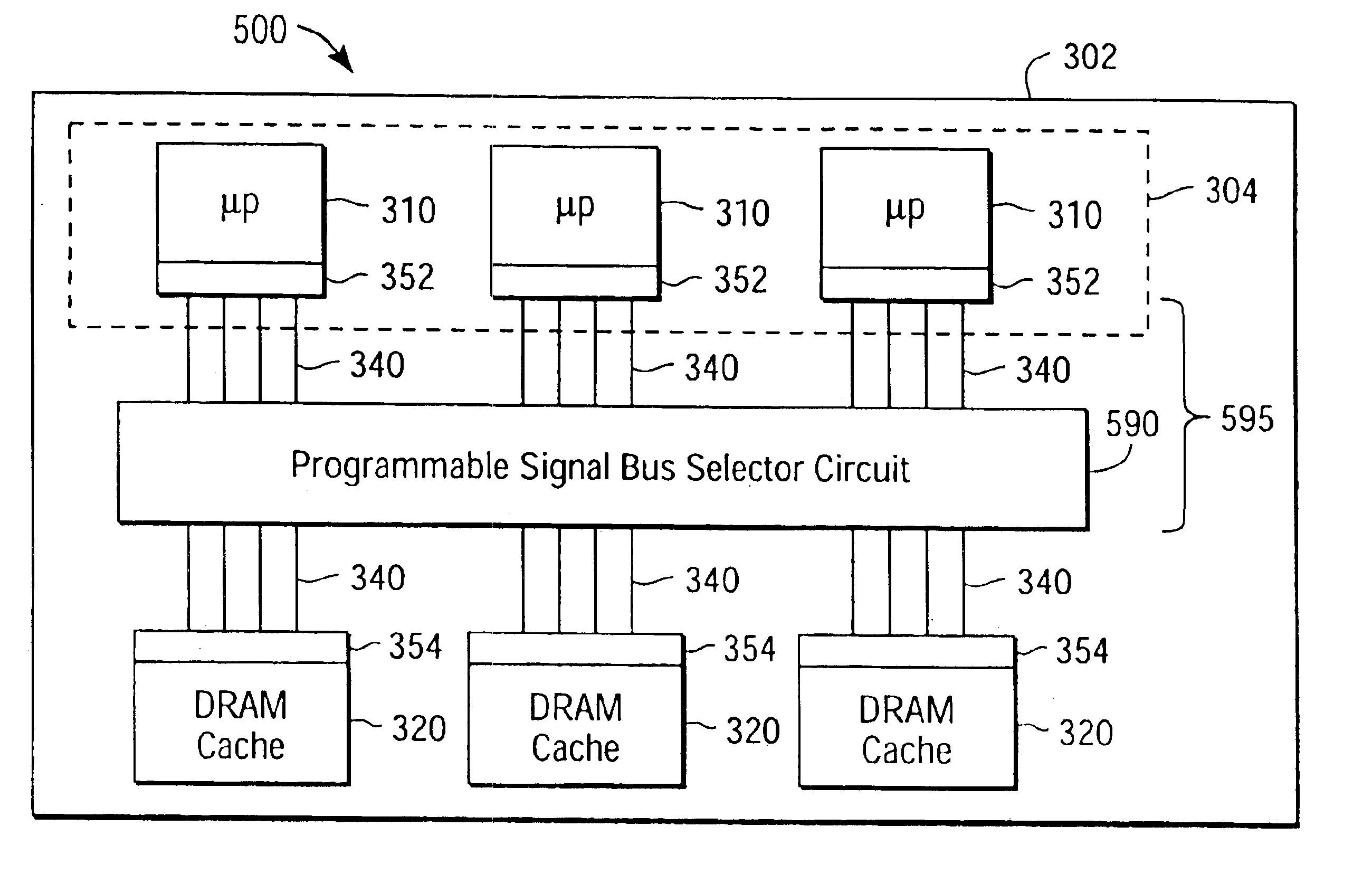
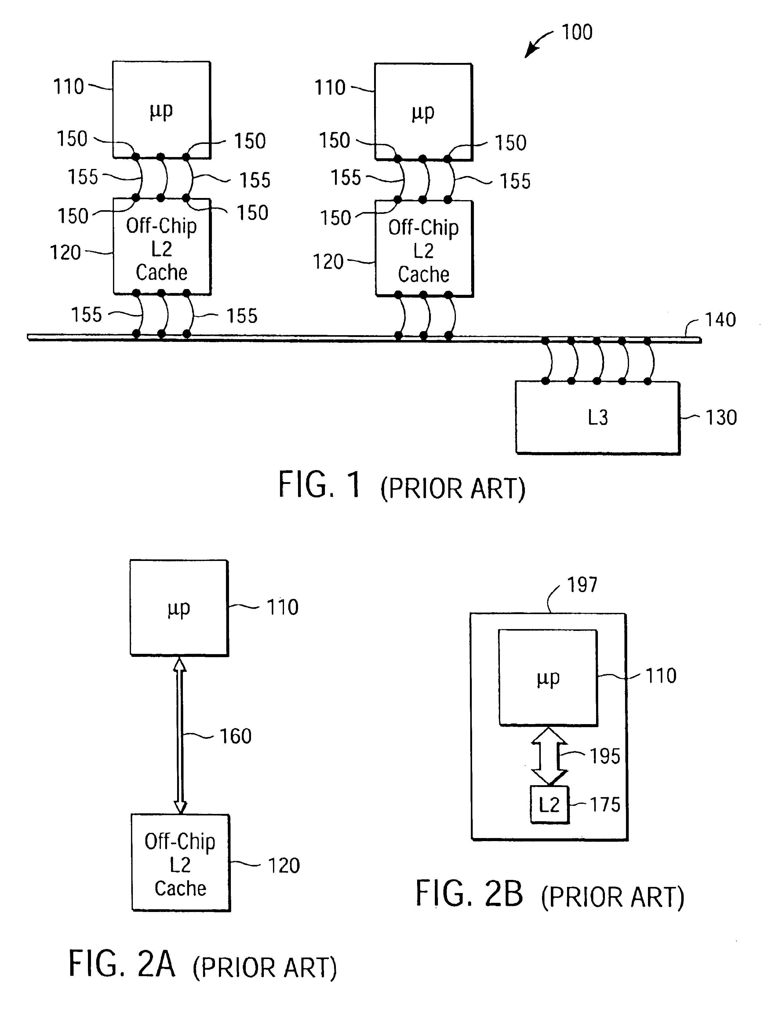
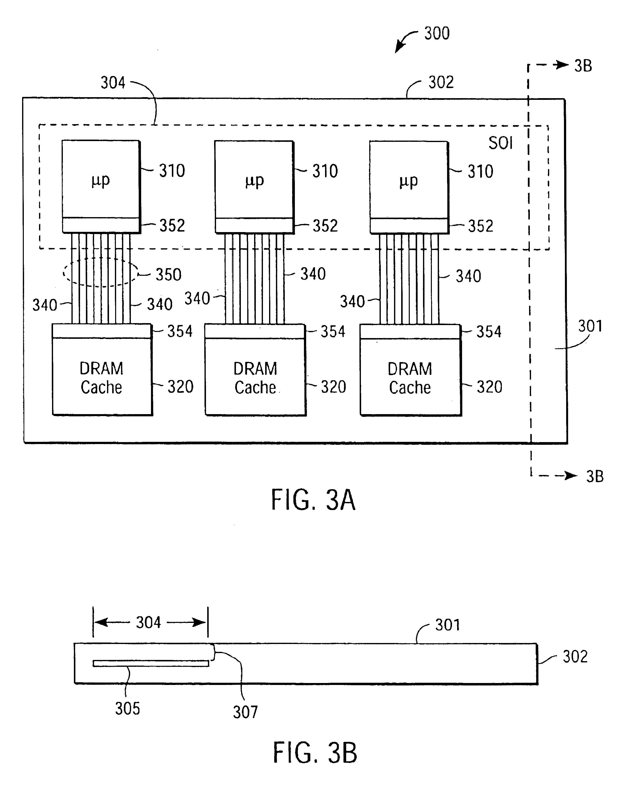
FIG. 3A is a block diagram illustrating a first embodiment of a chip 300 of the present invention. Chip 300 is an integrated circuit that is preferably formed on a conventional semiconductor substrate die size. Some details are omitted for the purposes of illustration. The inventors of the present application have recognized that recent advances in ultraviolet lithography, optical pattern correction, and phase-shift masking permit a greater than four-fold reduction in the size of high-speed microprocessors compared with microprocessors fabricated by conventional optical lithography. Consequently, as shown in FIG. 3A, chip 300 includes a plurality of micro...


PUM


Abstract

A multiprocessor integrated circuit is disclosed. A preferred embodiment of a multiprocessor chip has microprocessors formed on silicon-on-insulator regions and dynamic random access memory level-2cache memories or level-3 cache memories formed on bulk regions of the chip. A preferred embodiment includes a redundant architecture having a signal bus for coupling the microprocessors to the level-2 or level-3 cache memories in which the signal bus includes a programmable selector circuit for bypassing defective microprocessors or defective level-2 or level-3 cache memories.

Description

BACKGROUND OF THE INVENTION1. Field of the InventionThe present invention relates generally to multiprocessors, redundant circuits, and high-speed microprocessors. More particularly, the present invention is directed towards a multiprocessor chip with a redundant architecture having microprocessors fabricated on silicon-on-insulator and dynamic random access memory elements fabricated on bulk silicon.2. Description of Background ArtMultiprocessing is the use of more than one microprocessor to perform parallel processing. An apparatus to perform multiprocessing is typically called a multiprocessor or a parallel processor. There are several common control topologies for coordinating the action of the microprocessors and coupling the multiprocessor to a network. The microprocessors typically reside on separate chips with the system of microprocessors and memory units residing on one or more printed circuit boards. A signal bus is used to couple the microprocessors to different levels o...

Claims


Application Information

Patent Timeline
Patent Type & Authority Patents(United States)
IPC IPC(8): H01L21/70H01L21/762H01L21/84G06F11/20G06F12/08G06F12/16G06F15/16H01L21/822H01L27/04H01L27/12
CPCG06F12/0893H01L21/76243H01L21/84
Inventor MASLEID, ROBERT P.SCOTT, GREGORY S.
Owner FUJITSU LTD
Why Eureka
Try Eureka