Method for manufacturing nanostructured thin film electrodes

a thin film electrode and nanostructure technology, applied in photovoltaic energy generation, electrical equipment, electrolytic capacitors, etc., can solve the problems of limiting the choice of substrate materials, time and cost consumption in each step, and the method of forming nanostructured films is often time-consuming and cost-intensive. , to achieve the effect of shortening the process tim

Inactive Publication Date: 2005-04-19
FORSKARPATENT I UPPSALA
View PDF11 Cites 33 Cited by
  • Summary
  • Abstract
  • Description
  • Claims
  • Application Information

AI Technical Summary

Benefits of technology

[0021]The method of the invention is useful for providing a conducting substrate with a thin nanostructured porous film at a substantially shorter process time than has been possible previously. The reason for this is that no non-volatile substances are needed to mix with the electrode particle material, such substances generally used with previously known methods. Therefore, no long time, high temperature firing is needed to remove such non-volatile substances. In addition, no curing step is necessary.
[0022]Thus, with the method of the invention it is possible to use a wider range of substrate materials, i.e. materials having temperature properties that would make them unsuitable for a long lasting firing process, such as plastics. Further advantages with the method of the invention are described below.

Problems solved by technology

Actually, in addition to the firing process described above, conventional methods for forming nanostructured films include several steps, each step often rather time and cost consuming.
The firing step of conventional methods for forming nanostructured films also sets limits to the choice of substrate material.

Method used


Image

  • Method for manufacturing nanostructured thin film electrodes
  • Method for manufacturing nanostructured thin film electrodes
  • Method for manufacturing nanostructured thin film electrodes

Examples


experiment 1

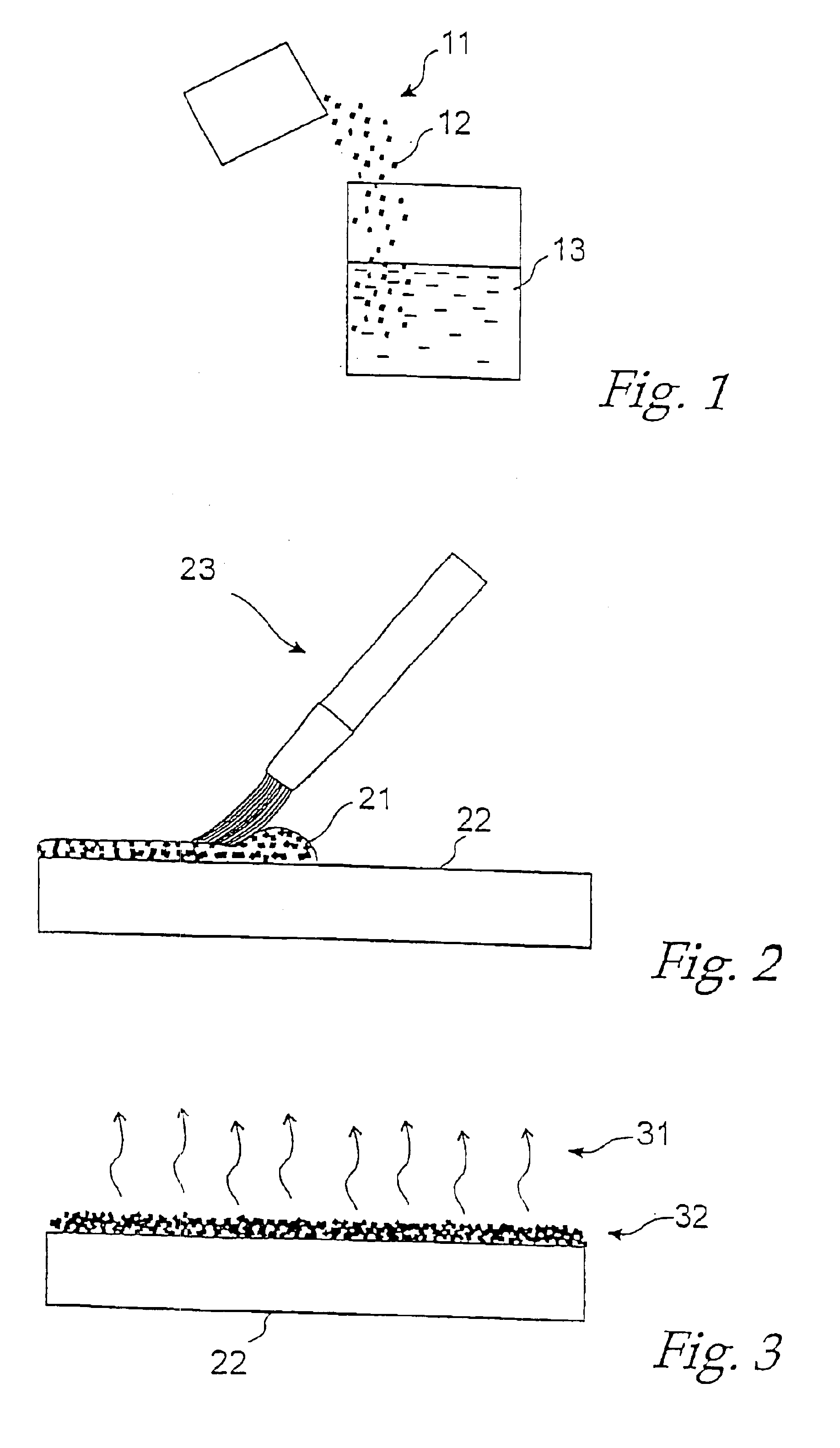
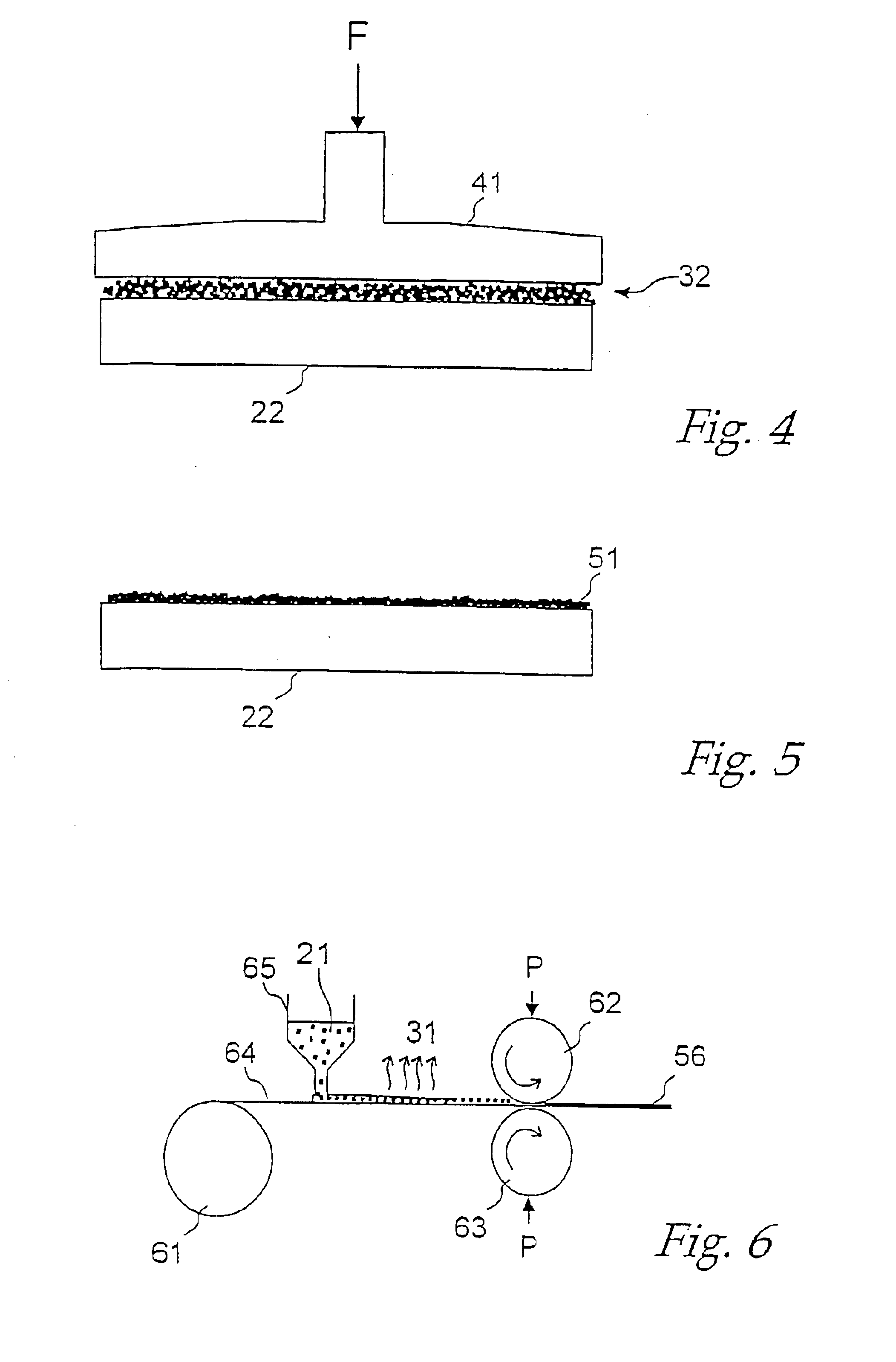
[0053]The conducting substrate was a “Tec 8” supplied by Hartford Glass Co, Inc. and consisted of a 10 cm×10 cm×3 mm soda lime glass sheet coated with a conducting layer of fluorine doped tin oxide of 8 ohm / cm2 resistivity. A suspension was prepared by adding 20% by weight TiO2 particles (Degussa P25) to ethanol. The suspension was applied to a thickness of 50 μm onto the conducting layer by brush application. The ethanol was allowed to evaporate to the air, and a 50 μm thick separating film of aluminum foil was draped on the particle layer. The assembly consisting of substrate, particle layer and separating film was placed between two planar stainless steel plates. A pressure of 300 kg / cm2 was applied on the assembly via the steel plates, to achieve a nanostructured film of appr. 55% porosity.

[0054]Then, the experiment above was repeated with new substrates, varying the pressure within 100-1000 kg / cm2. Thereby, the porosity achieved varied within appr. 50-60%, the higher the pressu...

experiment 2

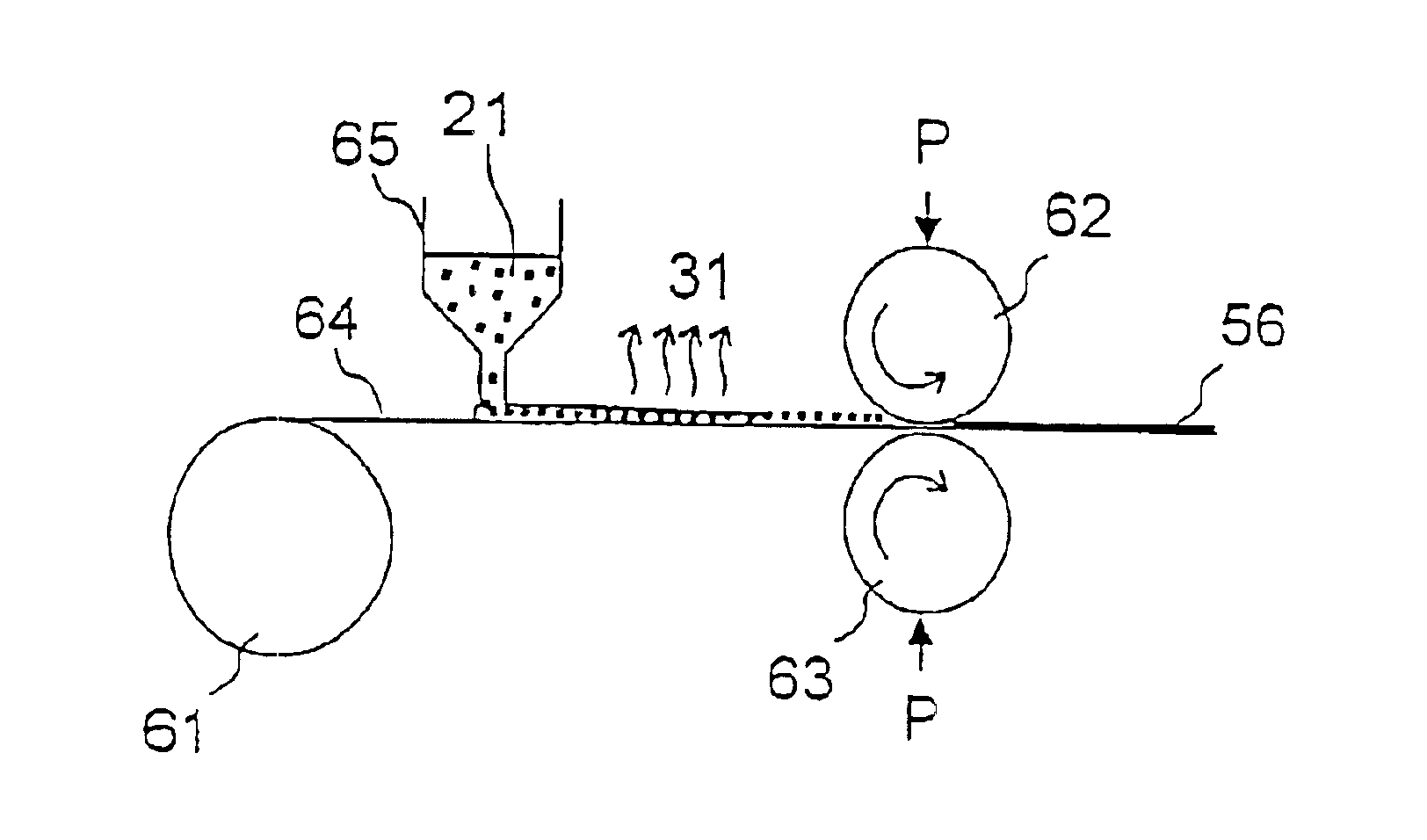
[0055]In another experiment a 5 cm×5 cm×0.2 mm conducting plastic substrate was used. The substrate was cleaned using a laboratory detergent “RBS 25” supplied from Labkemi. The preparation and application of the suspension was performed in the same way as the experiment described above. The ethanol was allowed to evaporate in air and a 25 μm thick separating film of low density polyethylene was draped on the particle layer. The film was compressed in the same manner as described in the experiment above, with the exception that the applied pressure was 1000 kg / cm2.

End of the Experiment 2

[0056]The method according to the invention to produce a nanostructured porous electrode has numerous advantages with respect to prior art methods. These advantages are mainly due to the fact that the method does not involve the use of a binder to temporarily or permanently bind the electrode particles. Such a binder, for example a polymer solved in a solvent or a wax, is both costly and requires a fi...

experiment 3

[0074]In another exemplifying experiment several stacked nanostructured layers were deposited onto a plastic substrate. The plastic substrate was a 5 cm×5 cm×0.175 mm “ITO-60” sheet supplied by IST (Innovative Sputtering Technology). A first layer of a nanostructured TiO2 film was deposited on the plastic film in the same manner as described in Experiment 2 above, with the exception that the suspension was applied to a thickness of 100 μm and the pressure applied was 1500 kg / cm.

[0075]In the next step, a suspension was prepared by mixing 40% by weight TiO2 powder (“Tioxide A-HR supplied by Huntsman) to ethanol. The second suspension was stirred with a magnetic stirrer for several hours and then applied onto the first layer to a thickness of 50 μm. The ethanol from the second layer was allowed to evaporate in air and a 25 μm thick separating film of low density polyethylene was draped onto the second particle layer. The second film was compressed by applying a pressure of 1000 kg / cm2....


PUM

PropertyMeasurementUnit
particle sizeaaaaaaaaaa
sizeaaaaaaaaaa
porosityaaaaaaaaaa

Abstract

A method for a binder-free manufacturing a nanostructured porous film, e.g. for use in solar cells, includes the steps of preparing a suspension of semi-conducting nanometer-sized particles in a volatile suspending agent (21), depositing the particle suspension on a conducting substrate, removing the suspending agent by evaporation (31), thereby leaving a particle layer on said substrate and compressing (P) the deposited particle layer for mechanical and electrical interconnection.

Description

CROSS REFERENCE TO RELATED APPLICATIONS[0001]This application is a continuation-in-part of application Ser. No. 09 / 991,715, filed on Nov. 26, 2001 now abandoned. Application Ser. No. 09 / 991,715 is the continuation-in-part of PCT International Application No. PCT / SE00 / 01060 filed on May 25, 2000 under 35 U.S.C. § 371. The entire contents of each of the above-identified applications are hereby incorporated by reference.TECHNICAL FIELD OF THE INVENTION[0002]The present invention relates to a method for manufacturing nanostructured thin film electrodes, and more specifically to a method for producing a nanostructured porous layer of a semi-conductor material on a substrate for use in an electrochemical or photoelectrochemical cell, such as a solar cell, display, battery etc.PRIOR ART[0003]The basic concept of nanostructured thin films is described by B. O'Regan and M. Grätzel in Nature, 353, 737 (1991), and by Grätzel et al in J. Am. Chem. Soc., 115, 6382 (1993).[0004]The application of...

Claims


Application Information

Patent Timeline
Patent Type & Authority Patents(United States)
IPC IPC(8): H01G9/20H01M4/00
CPCH01G9/2031H01M4/00Y02E10/542
Inventor LINDSTROM, HENRIKSODERGREN, SVENLINQUIST, STEN-ERICHAGFELDT, ANDERS
Owner FORSKARPATENT I UPPSALA
Why Eureka
Try Eureka