Method for manufacturing semiconductor device with crystallization of amorphous silicon

a technology of amorphous silicon and a semiconductor device, which is applied in the direction of semiconductor devices, basic electric elements, electrical appliances, etc., can solve the problems of not being suitable for a semiconductor device, not being able to match well with a silicon film, and tending to trap the charge of the film, so as to achieve high reliability and ensure the characteristics of the film to a certain degr

Inactive Publication Date: 2005-04-26
SEMICON ENERGY LAB CO LTD
View PDF56 Cites 36 Cited by
  • Summary
  • Abstract
  • Description
  • Claims
  • Application Information

AI Technical Summary

Benefits of technology

[0011]In view of the above-described circumstances, it is a primary object of the present invention to form a crystalline semiconductor film having a higher electrical characteristics and a higher reliability.
[0014]The use of a silicon nitride film prevents the silicon film from being oriented along the crystallographic (111) plane. Since crystallized silicon oxide has a diamond structure as a crystal silicon film does, a silicon film crystallized contacting silicon oxide tends to be oriented along the (111) plane due to the boundary energy therebetween. On the other hand, crystallized silicon nitride is cubic, and the matchability with a silicon film is not so good. Thus, by contacting the silicon nitride film, the amorphous silicon film can be crystallized without orienting along the particular plane.
[0027]The degree of crystallization (i.e. the proportion of the area of the crystallized region with respect to the entire area, as observed through a microscope) after heat treatment is in the range of from 20 to 90%. The maximum attainable amount of crystallization is about 97% by raising the heating temperature. However, the proportion of the amorphous component can be more effectively reduced to a negligible degree by irradiation by the above laser beam or intense light beam equivalent thereto.
[0029]In contrast to the above conventional laser process, crystallization in the process according to the present invention can be more readily effected because a crystal nucleus is present, and the crystallization process is less dependent on the cooling rate. Because a large part of the film is crystallized, the film characteristics can be assured to a certain degree even if a low energy density laser is used. Accordingly, in accordance with the present invention, an amorphous silicon film can be uniformly crystallized with a high reliability.
[0030]Instead of using a laser beam, non-coherent intense light, particularly infrared radiation, may be used. The majority of infrared radiation is not absorbed by glass, but is readily absorbed by thin film silicon. Accordingly, thin film silicon can be heated selectively without heating the glass substrate by the use of IR light. This process of radiating infrared light for a short period of time is called as rapid thermal annealing (RTA) or a rapid thermal process (RTP).

Problems solved by technology

If the ratio x is lower than 1.3, the film tends to trap the charge, and is not suitable for a semiconductor device.
On the other hand, crystallized silicon nitride is cubic, and the matchability with a silicon film is not so good.

Method used


Image

  • Method for manufacturing semiconductor device with crystallization of amorphous silicon
  • Method for manufacturing semiconductor device with crystallization of amorphous silicon
  • Method for manufacturing semiconductor device with crystallization of amorphous silicon

Examples


example 1

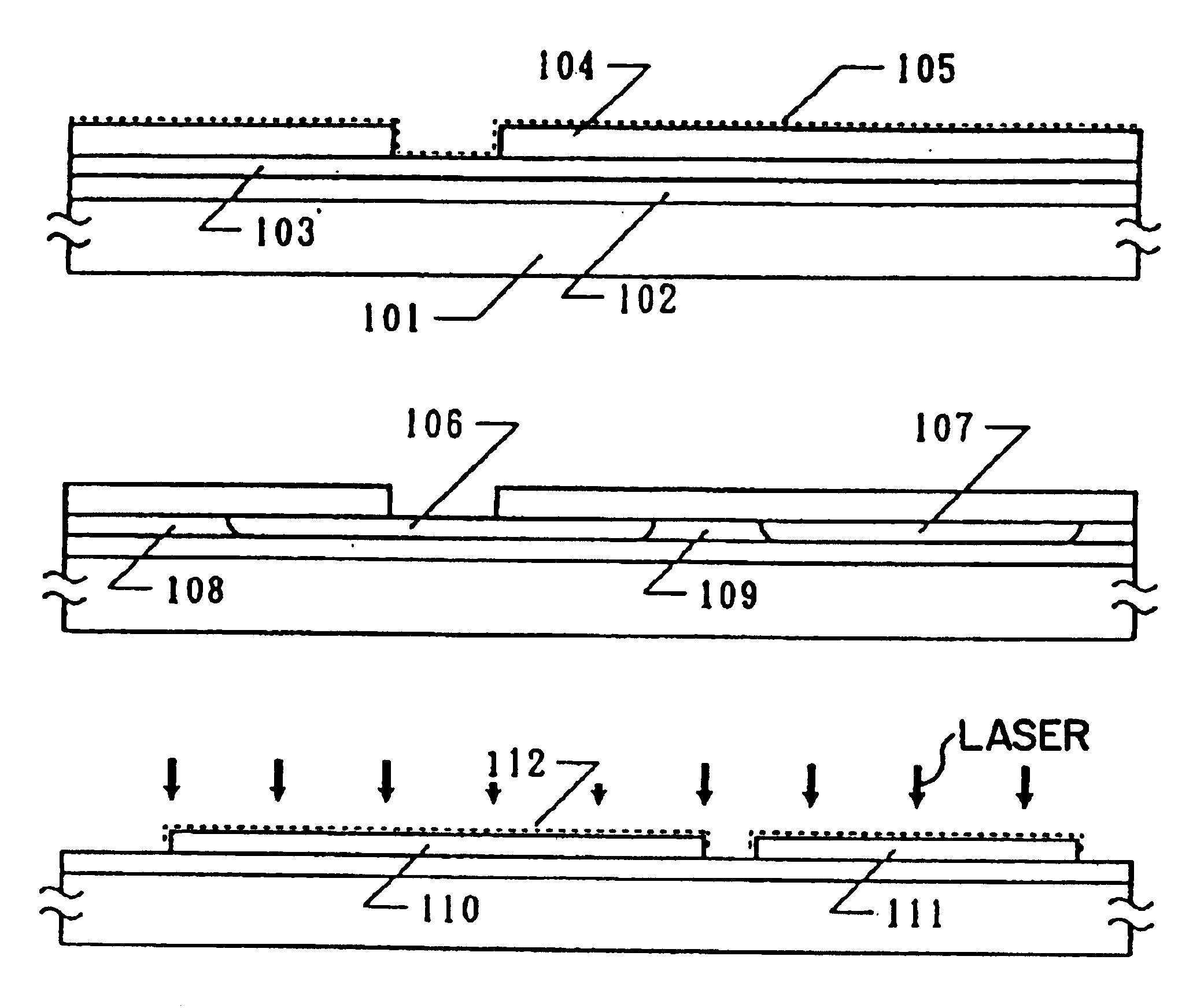
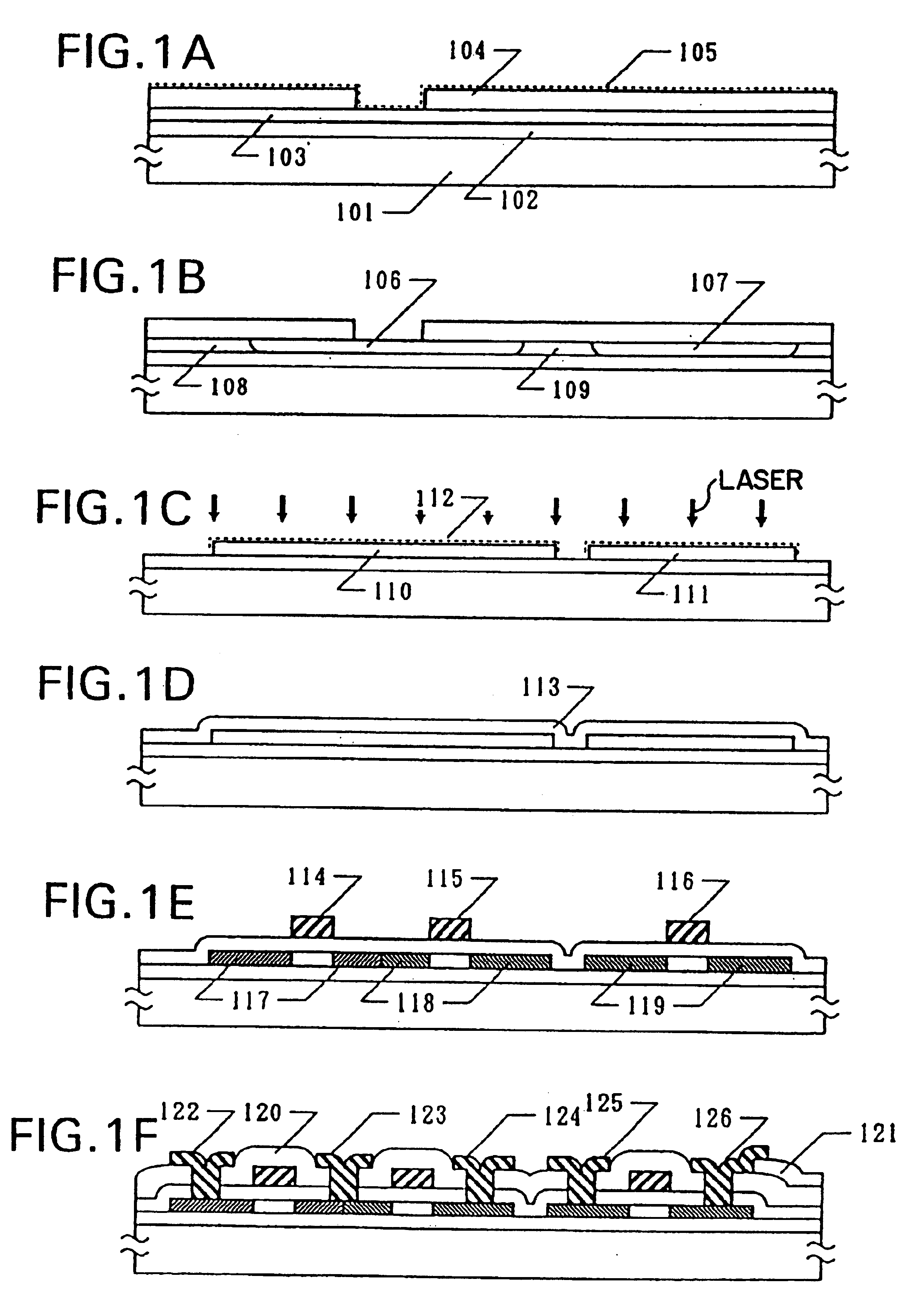
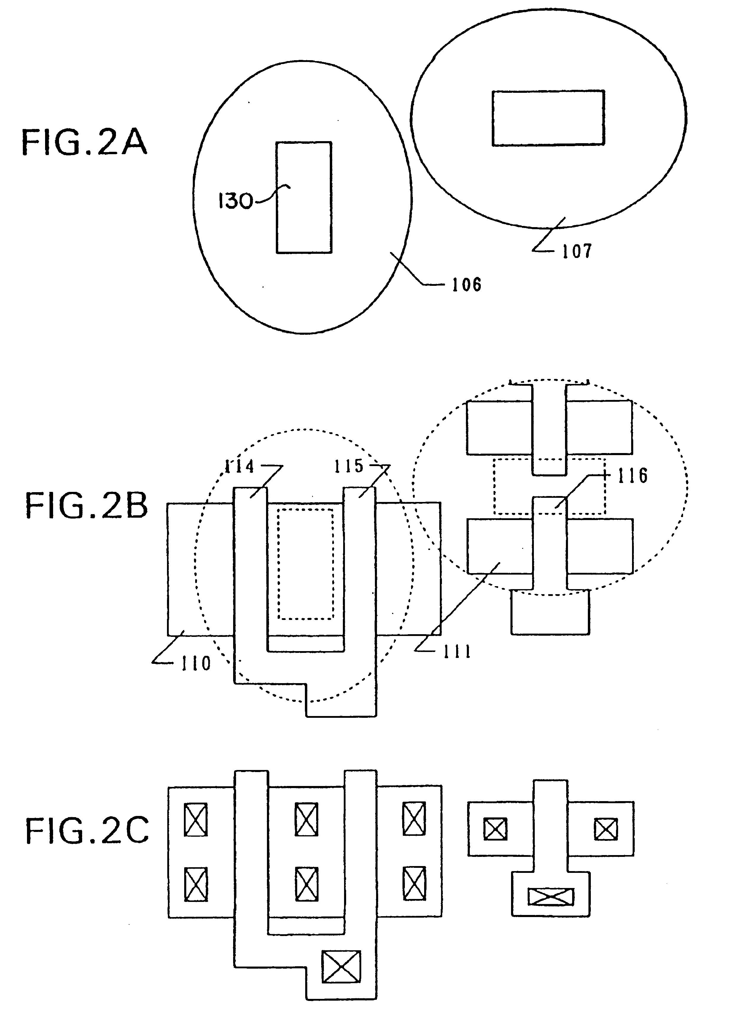
[0048]The present example refers to a process for fabricating a crystalline silicon film on the surface of a glass substrate. Referring to FIGS. 1A-1F, a Corning 7059 glass substrate 100 mm×100 mm in size and 1.1 mm in thickness was prepared. A silicon nitride film from 1,000 to 5,000 Å, for example, 2000 Å thickness was deposited as a base film 102 by sputtering or plasma CVD on the substrate 101. The stoichiometric ratio of nitrogen and silicon (nitrogen / silicon) was set to 1.3 to 1.35, preferably 1.32 to 1.34.

[0049]The silicon nitride film is formed, for example, by a plasma CVD with the following conditions:[0050]RF power: 13.56 MHz, 300 W[0051]Substrate Temperature: 300° C.[0052]SiH4 / NH3=30 sccm / 210 sccm[0053]Pressure: 0.3 Torr

[0054]Generally, when the temperature is higher, the concentration of hydrogen in the obtained film is reduced.

[0055]Then, an amorphous silicon film 103 was deposited to a thickness of 100 to 1,500 Å, for example, 800 Å by plasma CVD or LPCVD.

[0056]A sili...

example 2

[0073]The process for fabricating a semiconductor device according to the present example will be described below with reference to FIGS. 3A to 3F. A silicon oxide film 202 was deposited by a known method such as plasma CVD to a thickness of 1,000 to 5,000 Å, for example, 2000 Å as a base film on a Corning 7059 glass substrate 201 (10 cm×10 cm in size). An amorphous silicon film 203 was deposited by plasma CVD or reduced pressure CVD to a thickness of 1,000 Å.

[0074]After forming an ultra-thin silicon oxide film (not shown) on the surface of the amorphous silicon film using aqueous hydrogen peroxide, 5 ml of an acetate solution containing 25 ppm of nickel was dropped onto the oxidized surface of the amorphous silicon film in the same manner as in Example 1. Further, at this time, spin-coating was effected at 50 rpm for a duration of 10 seconds to form a uniform aqueous film over the entire surface of the substrate. After further retaining this state for a duration of 5 minutes, spin-...

example 3

[0085]A process for fabricating a semiconductor device according to a third example will be described below with reference to FIGS. 4A to 4F. A silicon oxide film 302 was deposited through plasma CVD to a thickness of 2,000 Å as a base film on an NH 35 glass substrate 301 (NH Technoglass Co., Ltd.). After depositing the base film, the structure was annealed in a temperature range of from 620 to 660° C. for a duration of from 1 to 4 hours, and was gradually cooled at a rate of 0.1 to 1.0° C. / minute, preferably from 0.1 to 0.3° C. / minute. The substrate was taken out when the temperature was cooled to 450-590° C.

[0086]An amorphous silicon film 303 was deposited by plasma CVD to a thickness of 300 to 1,200 Å, e.g. 500 Å. Then, a nickel acetate layer of 20 to 50 Å thick was formed by spin coating in the same manner as the foregoing Examples 1 and 2, using a mask 304 made of a silicon nitride film of 1,000 to 3,000 Å thick, e.g. 2,000 Å. As described in Example 1, it was necessary to form...


PUM

PropertyMeasurementUnit
temperatureaaaaaaaaaa
sizeaaaaaaaaaa

Abstract

A process for manufacturing a semiconductor device, particularly a thin film transistor, by using a crystalline silicon film having excellent characteristics. The process comprises forming a silicon nitride film and an amorphous silicon film in contact thereto, introducing a catalyst element capable of promoting the crystallization of the amorphous silicon film by heating the amorphous silicon film, thereby crystallizing at least a part of the amorphous silicon film, and accelerating the crystallization by irradiating the silicon film with a laser beam or intense light equivalent thereto.

Description

[0001]This application is a Continuation of Ser. No. 08 / 479,211, filed Jun. 7, 1995, now abandoned; which itself is a continuation-in-part of Ser. No. 08 / 391,580, filed Feb. 21, 1995 now U.S. Pat. No. 5,605,846.BACKGROUND OF THE INVENTION[0002]1. Field of the Invention[0003]The present invention relates to a method for manufacturing a semiconductor device using a crystalline semiconductor mainly comprising silicon. The silicon semiconductor obtained according to the method of the present invention is suitable for use in thin film transistors, thin film diodes and the like.[0004]2. Prior Art[0005]Thin film transistors utilizing a semiconductor thin film (referred to simply hereinafter as “TFTs”) are well known. TFTs are fabricated by forming a thin film semiconductor on a substrate and processing the thin film semiconductor thereafter. TFTs are widely used in various types of integrated circuits, and are particularly suitable in the field of electro-optical devices such as liquid cry...

Claims


Application Information

Patent Timeline
Patent Type & Authority Patents(United States)
IPC IPC(8): H01L21/02H01L21/70H01L21/20H01L21/336H01L21/84H01L21/77
CPCH01L21/02532H01L21/02667H01L27/1277H01L21/02686H01L29/66757H01L21/02672
Inventor OHTANI, HISASHIMIYANAGA, AKIHARUZHANG, HONGYONGYAMAGUCHI, NAOAKI
Owner SEMICON ENERGY LAB CO LTD
Why Eureka
Try Eureka