Semiconductor device, semiconductor wafer, semiconductor module, and a method of manufacturing semiconductor device

a semiconductor and semiconductor technology, applied in the direction of semiconductor devices, semiconductor/solid-state device details, electrical apparatus, etc., can solve the problems of difficult surface implementation, thin and easily deformed self, and inability to implement qfp, etc., to achieve the effect of high reliability and preferable mass production

Inactive Publication Date: 2005-05-03
RENESAS ELECTRONICS CORP
View PDF26 Cites 17 Cited by
  • Summary
  • Abstract
  • Description
  • Claims
  • Application Information

AI Technical Summary

Benefits of technology

[0034]In accordance with the present invention, the CSP having a package size which is the same as the chip size can be provided. A porous stress relaxing layer is used. The porous body is cut simultaneously when the semiconductor wafer is cut. Its end plane is inevitably exposed at the side plane of the package. Therefore, absorbed moisture at reflowing in mounting is released outside passing through the porous body. Accordingly, failures such as peeling off by vapor pressure of water can be prevented, and a CSP having a high reliabilit...

Problems solved by technology

However, implementation of the QFP is becoming difficult because of the increasing number of pins, since the connecting leads with the implementing substrate are concentrated at the periphery of the package, and the lead itself is thin and can be readily deformed.
The PGA is disadvantageous in a high density implementation, because the increasing processing velocity is difficult to attain electrically, since terminals of the PGA for connecting with the implementing substrate are slender and are concentrated so as to be extremely close to each other, and surface implementation is impossible, since the PGA package is a pin insertion type.
Accordingly, a problem occurred in that the package size of such a CSP became larger than the chip.
A CSP using chips cut in pieces experienced a problem in that it took a long time to manufacture the semiconductor device, because, after dicing the chips, each respective chip must be located correctly on the substrate, adhered thereon, connected electrically, and sealed.
A CSP using a resin substrate, such as a substrate made of pol...

Method used


Image

  • Semiconductor device, semiconductor wafer, semiconductor module, and a method of manufacturing semiconductor device
  • Semiconductor device, semiconductor wafer, semiconductor module, and a method of manufacturing semiconductor device
  • Semiconductor device, semiconductor wafer, semiconductor module, and a method of manufacturing semiconductor device

Examples


embodiment 1

(Embodiment 1)

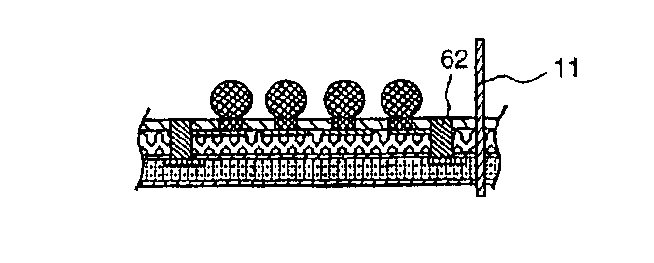
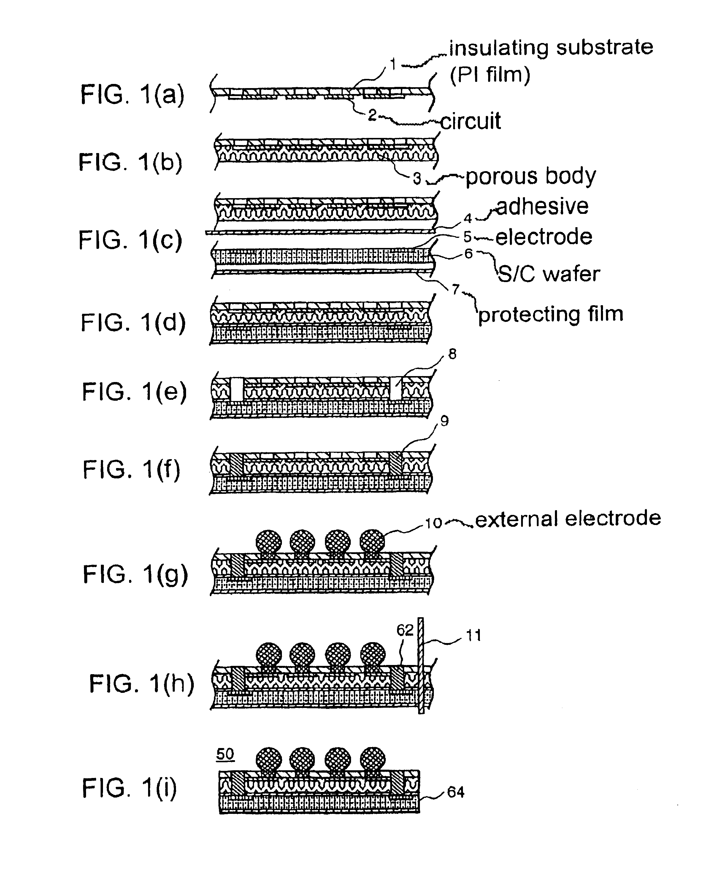
[0047]FIGS. 1(a) to 1(i) illustrate steps in the manufacture of a semiconductor device representing an embodiment of the present invention, and a semiconductor device obtained by the manufacturing steps is shown in FIG. 1(i).

[0048]In accordance with the manufacturing steps of FIGS. 1(a)-1(i), the semiconductor wafer and the semiconductor device of the present invention were prepared.

[0049]In the step of FIG. 1(a), a polyimide film (UB rex S: made by Ube Kosan Co.) 50 μm thick, whereon an epoxy group adhesive agent was applied, was used as the insulating substrate 1. Device holes were formed by punching in the insulating substrate 1. Electrolytic copper foil 18 μm thick was adhered to the polyimide film by heating and pressurizing with a roller at 150° C. After applying photosensitive resist (P-RS300S: made by Tokyo Ohka Co.) onto the electrolytic copper foil, it was baked at 90° C. for 30 minutes, and an etching mask was prepared by exposing and developing a pattern.

[0...

embodiment 2

(Embodiment 2)

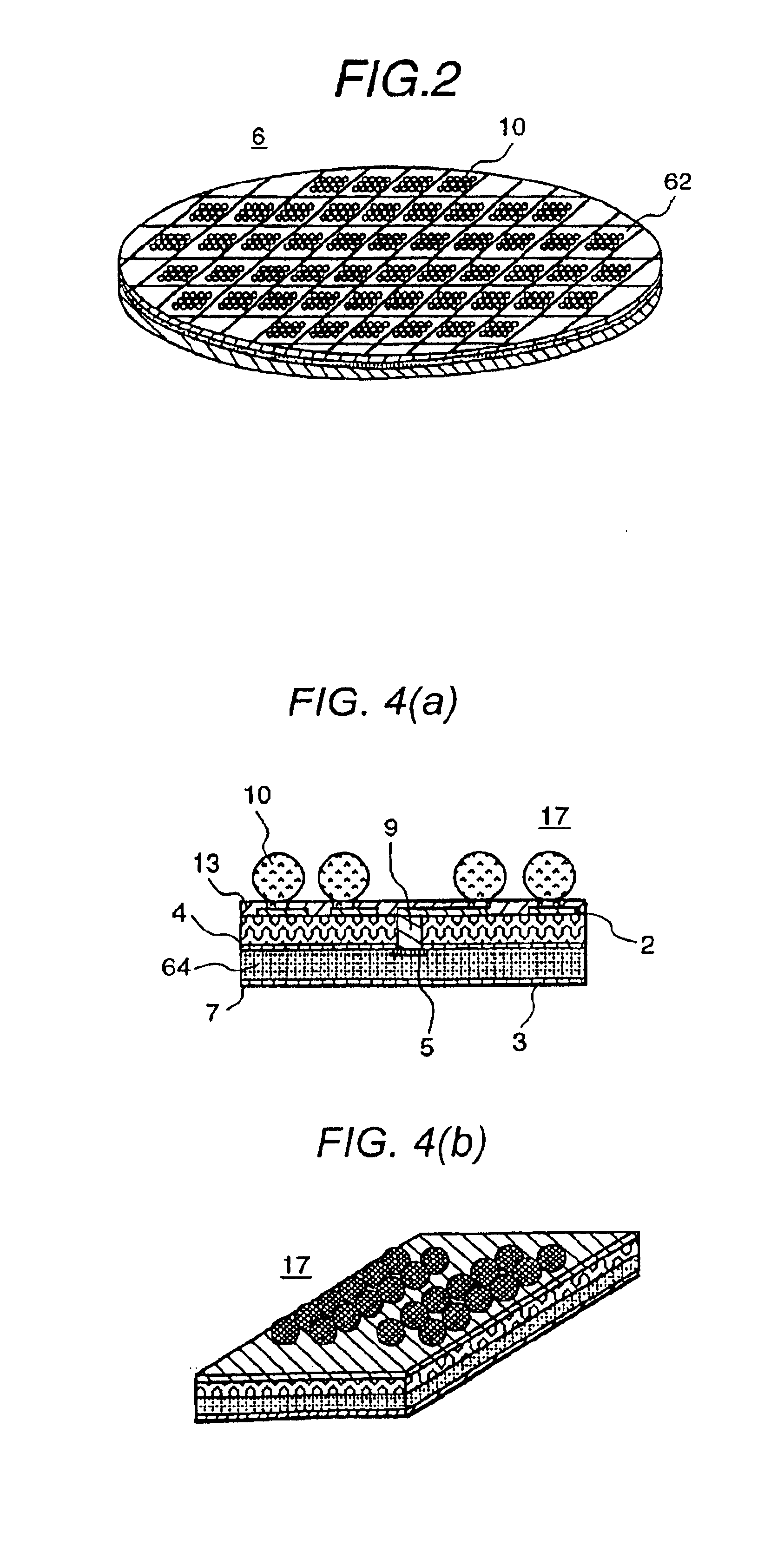
[0063]FIGS. 3(a) to 3(h) show steps in the manufacture of a semiconductor device representing another embodiment of the present invention, and a semiconductor device obtained by the manufacturing steps as shown in FIG. 3(h).

[0064]In accordance with the manufacturing steps of FIGS. 3(a)-3(h), the semiconductor wafer 6 and the semiconductor device 17 of the present invention were prepared.

[0065]In the step of FIG. 3(a), a porous body 3 made of polytetrafluoroethylene having a three dimensional network structure of 150 μm, which was prepared by a drawing method, the adhesive agent 4, the semiconductor wafer 8, and the wafer protecting film 7 were arranged as indicated. A semiconductor wafer 8, which was 4 inches in diameter and 525 μm in thickness, was used. The adhesive agent 4 and the wafer protecting film 7 were prepared by impregnating the adhesive varnish containing non-volatile component 35% (biphenyl type epoxy resin (YX-4000: made by Yuka Shell Co.) was dissolved ...

embodiment 3

(Embodiment 3)

[0076]FIG. 4(a) and FIG. 4(b) show a cross sectional view and a perspective view, respectively, of a semiconductor device representing another embodiment of the present invention. The semiconductor device was obtained by the following manufacturing steps.

[0077]After forming the via-holes by the same process as the embodiment 2, copper film was formed on the inner wall of the via-holes and the surface of the porous body by a vacuum deposition method. The subsequent processes were the same as used in the previous embodiment to manufacture the semiconductor wafer 6 and the semiconductor device 17.

[0078]The semiconductor device 17 was mounted on a mounting substrate, and a temperature cycle test in the range from −55° C. to −125° C. was performed. As the mounting substrate, a copper clad glass cloth base epoxy laminate FR-4 (MC-E-67: made by Hitachi Kasei Co.) was used. Furthermore, a reflow test at 240° C. for 5 seconds was performed after absorbing moisture in an environ...


PUM


Abstract

Semiconductor devices, semiconductor wafers, and semiconductor modules are provided, wherein: the semiconductor device has a small warp; damage at the chip edge and cracks occurring in a dropping test are scarcely generated; and the semiconductor device is superior in mounting reliability and mass producibility. The semiconductor includes a semiconductor chip 64; a porous stress relaxing layer 3 provided on the plane, whereon circuits and electrodes are formed, of the semiconductor chip; a circuit layer 2 provided on the stress relaxing layer and connected to the electrodes; and external terminals 10 provided on the circuit layer; wherein an organic protecting film 7 is formed on the plane, opposite to the stress relaxing layer, of the semiconductor chip, and respective side planes of the stress relaxing layer, the semiconductor chip 6, and the protecting film 7 are exposed outside on the same plane.

Description

BACKGROUND OF THE INVENTION[0001]The present invention relates to a semiconductor device comprising a chip size package of the type used for a high density mounting module, a multichip module, and the like, a method of manufacturing the same, and to a semiconductor wafer used for manufacturing the semiconductor device.[0002]Currently, in accordance with the current trend toward making electronic devices small, while retaining a high performance, semiconductor devices used therein are required to have a high integration, a high density, and to have a fast processing speed.[0003]Corresponding to such a requirement, the methods of manufacture of semiconductor devices have been changed from the pin insertion type to a surface implementing method for increasing the implementing density; and, in order to accommodate an increasing number of pins, packages, such as a DIP (Dual Inline Package), a QFP (Quad Flat Package), a PGA (Pin Grid Array), and the like, have been developed.[0004]However...

Claims


Application Information

Patent Timeline
IPC IPC(8): H01L21/02H01L23/50H01L21/50H01L21/60H01L21/301H01L23/52H01L23/28H01L21/46H01L23/12H01L23/48H01L21/48H01L29/40H01L23/31
CPCH01L23/3114H01L23/3164H01L23/3171H01L2224/45144H01L2224/73265H01L2224/32225H01L2924/01322H01L2924/01087H01L24/48H01L2924/3025H01L2924/30107H01L2924/15311H01L2924/12044H01L2224/1147H01L2224/16H01L2224/48227H01L2924/01078H01L2924/01079H01L2924/00H01L24/05H01L24/45H01L2224/02379H01L2224/05001H01L2224/05008H01L2224/05026H01L2224/05569H01L2224/05571H01L2224/06131H01L2224/0615H01L2924/00014H01L2924/12042H01L2924/181H01L2224/05599H01L2224/05144H01L2224/05147H01L2924/00012H01L23/52
Inventor OGINO, MASAHIKOUENO, TAKUMIEGUCHI, SHUJINAGAI, AKIRASATOH, TOSHIYAISHII, TOSHIAKIKOKAKU, HIROYOSHISEGAWA, TADANORITSUYUNO, NOBUTAKENISHIMURA, ASAOANJOH, ICHIRO
Owner RENESAS ELECTRONICS CORP
Why Eureka
Try Eureka