Method of patterning the surface of an article using positive microcontact printing

a positive type, microcontact technology, applied in the direction of nanoinformatics, photomechanical equipment, instruments, etc., can solve the problems of slow and expensive e-beam lithography, inability to achieve high-quality patterns, so as to reduce both cost and process complexity, and improve mechanical stability.

Inactive Publication Date: 2005-05-17
IBM CORP
View PDF6 Cites 23 Cited by
  • Summary
  • Abstract
  • Description
  • Claims
  • Application Information

AI Technical Summary

Benefits of technology

[0028]According to a second aspect of the present invention is provided a printing process of the positive type wherein the structures formed on the stamps have better mechanical stability.
[0029]According to a third aspect of the present invention is provided a microcontact printing process of the positive type which allows to fabricate more stable patterns on the stamp without requiring the use of a reactive ion etcher (RIE), thereby reducing both cost and process complexity.
[0030]According to a fourth aspect of the present invention is provided a microcontact printing process of the positive type wherein high-resolution lines on a substrate are produced using high-resolution grooves on the stamp, allowing easier unmolding.
[0031]According to a fifth aspect of the present invention is provided a microcontact printing process of the positive type which allows a faster print operation on an object for higher manufacturing throughput.
[0032]According to another aspect of the present invention is provided a microcontact printing process of the positive type which allows a print operation on the object to be substantially homogeneous all across the object surface.
[0033]According to yet another aspect of the present invention is provided a microcontact printing process of the positive type that allows to pattern a thiol indirectly on a surface which is not compatible with the stamp material.

Problems solved by technology

Because, photolithography is usually performed under very clean and controlled environments, it is an expensive but powerful technique well suited for mass fabrication of structures and devices having lateral dimensions ranging from a few millimeters to less than 100 nanometers.
The contrast and resolution of patterns made using photolithography should be as high as possible because it is not desirable to have some photoresist left in regions where the substrate should be etched away.
Since e-beam lithography is a slow and expensive patterning technique, it is important to use either a positive type or negative type of resist depending upon the application to minimize the writing time.
This technique is interesting because it can yield an overall negative process using a positive resist, but it has an inherent limited resolution and contrast.
Second, a SAM is usually thin, about the length of one of its molecule or just a few nanometers thick.
This work is severely constrained, however, by the instability of the SAM before it is photopatterned.
This SAM is formed of short molecules which are sensitive to ambient light and unstable under standard laboratory conditions.
This SAM has limited thermal stability, additionally.
This resulted in a poor contrast of the patterns of the etched substrate.
The same problems occur: the first SAM is too unstable under ambient conditions and tends to be exchanged by too many molecules during the formation of the second SAM in undesired areas.
Mechanical stability of the patterns on micropatterned stamps is a major problem.
Stamps having small structures separated by long gaps (zones which should not come into contact with the substrate) are mechanically unstable.
This can interfere with the layout of an electrical circuit or can create light absorbing zones where maximum transmission of light is desired, for example.
Fabricating harder stamps might not be desirable in particular for printing on rough substrates or on substrates having already some structures present before printing because in these cases, the stamp would be too hard to deform enough to match well the topography of the substrate.
However, in this case, a deep mold would be required, which might be difficult or expensive to fabricate.
High-resolution lines on a stamp can be difficult to unmold, because lines and posts on PDMS stamps can break and detach when a stamp is peeled off a high-resolution master or if the structures are large but have a unfavorable geometry.
This can be another major problem for patterning a substrate because the SAM should be as homogenous and protective as possible everywhere.
It is relatively easy to have a homogeneous printing time with these tools but it is difficult to have long enough printing time to form well protective SAMs because the contact between the stamp and the substrate takes place only in a small area at a time.
In addition, it seems difficult, if not impossible, to print a molecule to form a SAM which is not compatible (swells, damages, cannot be inked, .
This is unfortunate when the molecules forming the best monolayer on the substrate for a given application might not be forming a good or practical ink.
Finally, the above MCP process lacks flexibility.
In summary, the above described negative MCP process has the inconveniences and inherent limitations that are recited hereunder.a. First of all, some micropatterned stamps are mechanically unstable because some of their features collapse during printing and areas of the stamp which should not come into contact with the substrate in fact print.
Because, a reactive ion etcher is employed for this purpose, standard negative MCP processes are complex and expensive.b. High-resolution lines on a stamp can be difficult to unmold.c. Large substrates are long to print and the printing time is not homogeneous across the substrate.
Consequently, with conventional negative MCP processes, SAMs printed over large substrates have different quality which leads to problems during the etch step subsequently performed.d.
It seems difficult, if not impossible, to print a thiol which is not compatible with a stamp material.e.

Method used


Image

  • Method of patterning the surface of an article using positive microcontact printing
  • Method of patterning the surface of an article using positive microcontact printing
  • Method of patterning the surface of an article using positive microcontact printing

Examples


first embodiment

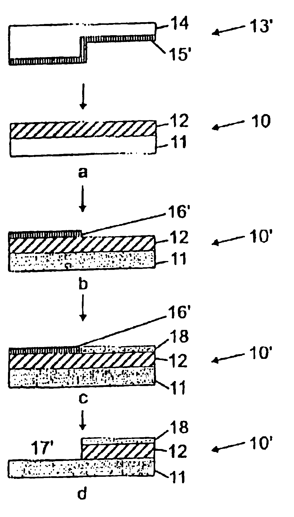
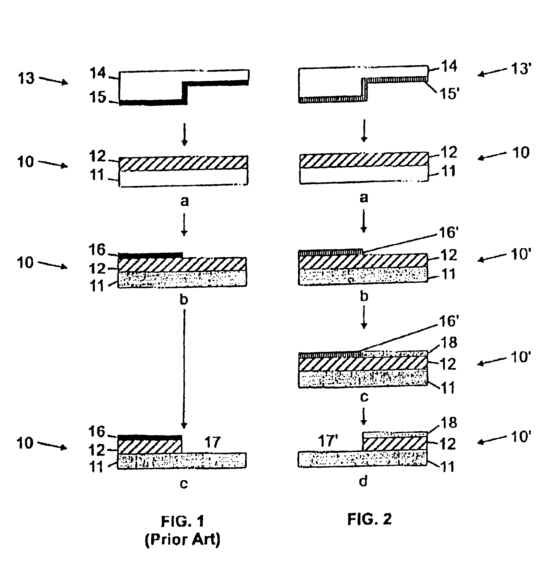
[0050]A first embodiment is conducted with a same object as used in the standard negative MCP described above by reference to FIGS. 1a-1c. Object 10 thus still comprises a 20-nm-thick Au layer 12 which is evaporated using an electron-beam evaporator on a silicon wafer substrate 11 having a film (20 nm) of native oxide. A 1-nm-thick layer of Ti which plays the role of an adhesion promoter is also evaporated therebetween as standard. In FIG. 2a, there is shown a micropatterned stamp 13′ comprising a PDMS body 14 inked with a 0.3 mM solution of pentaerythritol-tetrakis (3-mercaptopropionate) (abbreviated PTMP) in ethanol for 1 min to form the stamping pattern 15′. After the stamp 13′ is blown dry, e.g. using N2, it is applied onto the substrate surface with the layer 12 and the conformal contact between the stamp 13′ and the layer 12 ensures substantially homogeneous transfer of PTMP molecules to the layer 12. The print lasts for 30 s before the stamp 13′ is removed resulting in the fo...

second embodiment

[0052]The second embodiment demonstrates the feasibility to produce patterns in a Cu layer. In this case, the object 10 now comprises a silicon wafer as the substrate 11 having a 1-nm-thick titanium layer formed thereon as an adhesion promoter coated with a 100-nm-thick copper (Cu) layer 12 deposited in an electron-beam evaporator. The high conductivity of Cu makes it a good material for forming conductive patterns atop semiconductor structures. Because Cu exposed to ambient conditions tends to oxidize, the 100 nm thick copper (Cu) plated substrate is first immersed in 4% HCl in deionized (DI) water for 10 s to remove native copper oxide, then removed. Next, the object 10 is copiously rinsed with DI water and dried with a stream of N2. Now, according to the present invention, the PDMS stamp 14 is inked with a 0.2 mM solution of PTMP in ethanol for 1 min, to form a stamping pattern 15′ thereon, as shown in FIG. 2a. The Cu layer 12 is printed with the stamp 13′ forming the first SAM 1...

third embodiment

[0053]A third embodiment demonstrates the possibility of forming patterns on the 100-nm length scales. In this case, object 10 consists of a silicon wafer (having a 1 nm thick titanium layer formed thereon as an adhesion promoter) coated with a 50 nm thick copper (Cu) layer 12 deposited in an electron-beam evaporator. The Cu surface is treated as it is done in the previous example for removing the native oxide present on the Cu surface. Then, according to the present invention, the PDMS stamp 14 is inked with a 0.1 mM solution of PTMP in ethanol for 1 min, to form stamping pattern 15′, as shown in FIG. 2a. The Cu layer 12 surface is printed with the stamp 13′ forming the first SAM 16′, shown in FIG. 2b. Object 10 is then immersed in a 0.6 mM solution of eicosanethiol (ECT) in ethanol for 2 min. The purpose of this step is to deposit eicosanethiol in the unprinted areas as apparent in FIG. 2c and form the second SAM 18. Object 10 is removed from the bath, rinsed with ethanol and drie...


PUM

PropertyMeasurementUnit
pHaaaaaaaaaa
pHaaaaaaaaaa
thickaaaaaaaaaa

Abstract

There is disclosed a method of patterning an article (10) including a layer (12) of copper formed onto an insulating substrate (11) using a positive microcontact printing (MCP) process. In a preferred embodiment where the metal is copper (Cu) and the substrate is a silicon wafer, the method includes removing the native oxide presents on the Cu in a solution of HCl. Then, a stamp (13′) having a patterned polydimethylsiloxane (PDMS) body (14) is linked with a 0.2 mM solution of pentaerythritol-tetrakis(3-mercaptopropionate) (PTMP) in ethanol for 1 min, to form the inking layer (15′). The stamp is applied on the Cu layer to print a first self-assembled monolayer (SAM) (16′) according to a desired pattern. The article is dipped in a solution of ECT which is then adsorbed only in the non printed regions, forming a second SAM (18) in a configuration that is complementary to the desired pattern. Finally, the printed areas of the Cu layer are removed using a peroxodisulfate etch bath.

Description

FIELD OF THE INVENTION[0001]The present invention relates to advanced lithography techniques and more particularly, to a microcontact printing process of the positive type and a method of patterning the surface of an object using said microcontact printing process of the positive type.BACKGROUND OF THE INVENTION[0002]Conventional lithography encompasses a number of techniques. Photolithography is an important technique that is widely used for the fabrication of microstructures, such as semiconductor devices. Basically, it is usually performed as follows. First, a solution of photosensitive polymeric type of material dissolved in a solvent is spin-coated onto a substrate to form a homogeneous layer of a controlled thickness. Second, the substrate covered with the photoresist layer is heated to eliminate most of the solvent and the photoresist is selectively exposed to light using a patterned optical mask to block light where desired. Ultraviolet light is usually employed and its inte...

Claims


Application Information

Patent Timeline
Patent Type & Authority Patents(United States)
IPC IPC(8): B81C1/00G03F7/00G01Q60/00G01Q70/00
CPCB81C1/0046G03F7/0002B82Y30/00B82Y40/00B82Y10/00B81C2201/036C23F1/02
Inventor DELAMARCHE, EMMANUELGEISSLER, MATTHIASWOLF, HEIKO
Owner IBM CORP
Why Eureka
Try Eureka