Multibit non-volatile memory and method

a non-volatile memory and multi-bit technology, applied in the field of multi-bit non-volatile memory and methods, can solve the problems of reducing the chei efficiency and corresponding programming speed, and it is becoming difficult and harder to generate these voltages on-chip from a high-voltage generator or charge pumping circui

Inactive Publication Date: 2005-05-24
INTERUNIVERSITAIR MICRO ELECTRONICS CENT (IMEC VZW) +1
View PDF13 Cites 153 Cited by
  • Summary
  • Abstract
  • Description
  • Claims
  • Application Information

AI Technical Summary

Benefits of technology

[0059]The first and second junction can be formed selfaligned to said locations for storing charge and the select gate can separate said locations for storing charge. The vertical cross-section of the charge storage locations parallel with said wordline, can have a uniform thickness, e.g. have a rectangular cross-section. This is an advantage of the present invention as conventional techniques produce sloping surfaces.
[0060]A first gate dielectric can separate the first polysilicon layer from said semiconductor surface, and a second gate dielectric can separate said second polysilicon layer from said semiconductor surface. The first and second charge storage gates can be floating gates and charge can be stored within said first polysilicon layer of each charge storage gate. In accordance with an embodiment of the present invention a first and a second program gate can be formed in said second polysilicon layer, parallel with said wordline, and said first and said second program gates respectively can overlap said first and said second charge storage gates.
[0061]Said first polysilicon layer need only be present underneath said wordline formed in said second polysilicon layer.
[0062]In accordance with embodiments of the present invention said first and second charge storage gates can be program gates and said first dielectric can then comprise a charge storing dielectric. Said charge storing dielectric can be a nitride or a polysilicon with nanocrystals or similar materials, said nitride or polysilicon with nanocrystals or similar materials being capable of holding charge in selected regions thereof and said first polysilicon layer is used as program gate.
[0063]Second dielectric can be a charge storing dielectric and said charge storing dielectric can be a nitride or a polysilicon with nanocrystals or similar materials, said nitride or polysilicon with nanocrystals or similar materials being capable of holding charge in selected regions thereof.
[0064]The present invention also provides a method for forming a multibit non-volatile memory cell structure comprising:

Problems solved by technology

This supply voltage scaling is known to degrade the CHEI efficiency—and hence the corresponding programming speed—considerably.
Due to the high power needed to trigger the CHEI it becomes harder and harder to generate these voltages on-chip from a high voltage generator or charge pumping circuit.
Further improvement is, however, limited by tunnel-oxide scaling limits and by the very high voltages (˜15V) needed on chip for FNT, both compromising device reliability and process scalability.
However, the solutions found suffer from a number of significant disadvantages that will be discussed below in more detail.
It is, however, very difficult to control this selective etching operation, as for example the width of the spacer remaining after etching determines the effective channel length during programming and this parameter should be tightly controlled.
Since the select gate controls only a short portion of the channel, it is not straightforward to switch off the transistor channel in some cases, e.g. when reading / writing a particular cell the select gates of the (erased) cells sharing the same bitline have to be able to reduce their channel current to zero in order to prevent leakage currents and / or unwanted programming in the array.
Therefore, the injection efficiency is compromised by isolation requirements.
The main problem with these devices, however, is the difficulty of contacting the cells in a large array of memory cells.
Also, variations in sheet resistance, due to variations in spacer profile and / or doping, can lead to poor cell uniformity in large arrays which typically shows up as a severe manufacturability issue.
However, the major drawbacks of the sidewall gate device are still present in the memory cell described in this patent;
As already mentioned above, the thickness of the polysilicon, which determines the width of the spacer, is usually smaller than the minimum feature size, which compromises the hard-off situation which is highly desired in a memory array.
This makes the leakage problem during read-out even more critical.
The major difference with the above discussed prior art is the absence of a sidewall gate.
It is known to one skilled in the art that such a processing scheme introduces considerable complexity which makes it difficultto use in an embedded memory application.
This restriction compromises scaling—in general—and also—more in particular—decreases the injection efficiency which is directly linked to the thickness of this spacing as explained extensively by J. Van Houdt et al. in IEEE Transactions on Electron Devices, vol.39, no.5, May 1992.
The split gate structure suffers from an inherent misalignment problem, since the second poly (control gate) is always slightly misaligned with respect to the first poly (floating gate).
This misalignment does not scale proportionally to the feature size of the technology, and, therefore, introduces larger non-uniformities in programming behaviour and in read current when scaling down.
In the case pending European patent application EP 1096572 A1 claiming priority of U.S. pending patent application Ser. No. 09 / 696,616 also the gate coupling ratio is subject to a misalignment error further increasing the spread on device characteristics.
This latter sensitivity can be solved by completely encapsulating the floating gate by the control gate but this is at the expense of cell area and reliability since then the oxide between wordline and bitline needs to withstand the stress of both gate and drain voltages during program / erase conditions.
A second major scaling problem is the requirement of having a separate self-aligned drain junction: the mask for this implant should cover part of the floating gate to make sure that the implant is only present in a self-aligned way at the drain end of the channel and not at the source side of the floating gate.
As explained above, poly spacer technology, as a self-aligned process, has been extensively tried out in order to circumvent these problems, however, without any commercial success so far.
However, both structures suffer from major drawbacks:
When using a triple poly layer approach (U.S. Pat. No. 5,278,439), the device suffers from the same drawbacks as the related U.S. Pat. No. 5,280,446, which has already been discussed above.
Only the misalignment issue is resolved at the expense of very complicated processing.
When using a poly spacer technology as in the Halo device, the device suffers from all major problems related to poly spacers as discussed above (U.S. Pat. No. 5,338,952).
Some additional drawbacks of such a spacer technology are for example poor interconnect properties causing yield and manufacturability problems (spacer uniformity in terms of shape, width, thickness, doping, .
This will affect the device performance considerably unless the thickness of the polysilicon layer is constant over the entire channel area.
Also, the spacer is only 80 nm wide in a 0.25 μm technology and can, therefore, not easily be controlled.
The problem with this configuration is that the spacing between both spacers then needs to be defined from an additional sacrificial layer.
This is detrimental for device performance and reliability.
), however at the expense of a complicated and therefore expensive process.
With respect to the previously discussed prior art, as far as it is known, neither poly spacer technologies, nor the dual bit triple poly layer approach mentioned above, have made it into production because of major manufacturability and yield problems, related either to the spacer itself, and / or to the third poly layer.

Method used


Image

  • Multibit non-volatile memory and method
  • Multibit non-volatile memory and method
  • Multibit non-volatile memory and method

Examples


first embodiment

[0113]Table 1: exemplary operating voltages for the memory array of FIG. 4b using source-side injection for programming

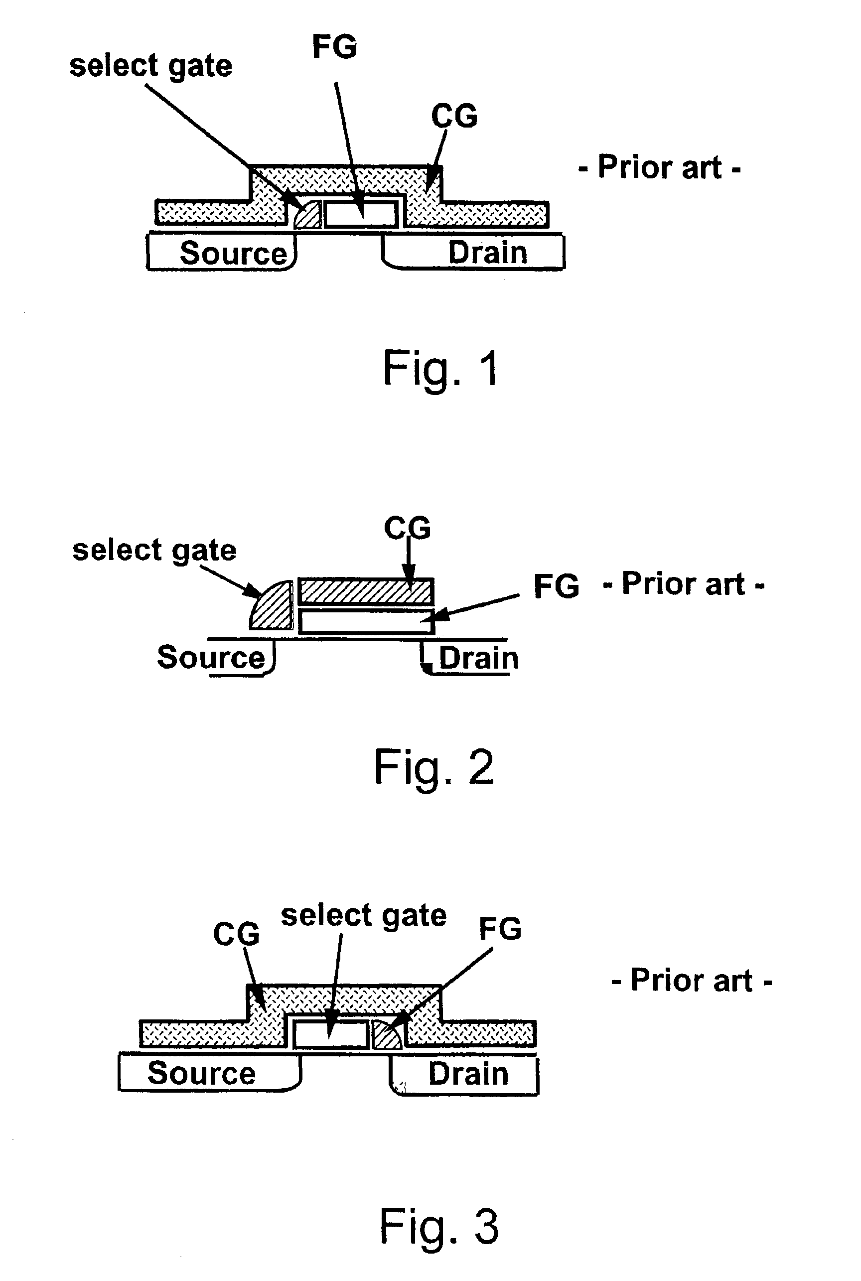
[0114]The device operates in a similar way to that of the HIMOS® devices described in the U.S. Pat. No. 5,583,811, if considering the program line (PL) of the opposing bit, i.e. the bit of the dual bit that is not programmed, as a transfer gate which is merely biased above the threshold-voltage window in order to access the addressed bit regardless of the value of the opposing bit. This explains the value of 3V in the table of operating voltages below: the threshold voltage is typically changed between −2.5V and +1 or 2V for HIMOS® and, therefore, 3V is sufficient in order to turn on the channel which is in series with the addressed bit in both read and write operations.

[0115]According to an aspect of the present invention, the problem concerning misalignment on the control gate channel length of the split-gate structure is avoided and the cell can be scaled down to...

second embodiment

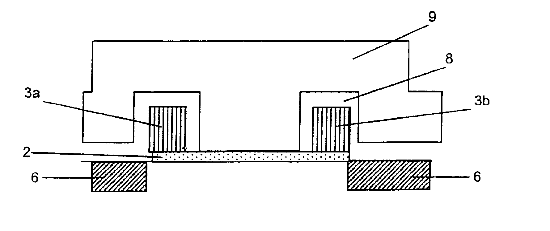
[0130]In another embodiment of the present invention an alternative to the method of the second embodiment is illustrated by FIGS. 5h-l. In the former embodiment, the width of the gate formed in the first polysilicon layer 3 is determined by the width of the spacer 5 formed in the second hardmask 5. As outlined above, this spacer 5 width is not determined by the lithographic process used, but is a function of layer thickness and etch processes. As illustrated in FIG. 5e the junction constituting the bitline 6 is then formed selfaligned to this floating gate 3a-b formed in the first polysilicon layer 3.

[0131]In a simplified process flow the floating gate FG 3a-b is formed using known patterning processes, see “Microlithography, Science and Technology”, J. R. Sheats et al. Marcel Decker, 1998. As shown in FIG. 5h a first polysilicon layer 3 is formed on top of the dielectric layer 2. The dielectric layer may for example be an ONO layer. As shown in FIG. 5i the width of the patterned f...

third embodiment

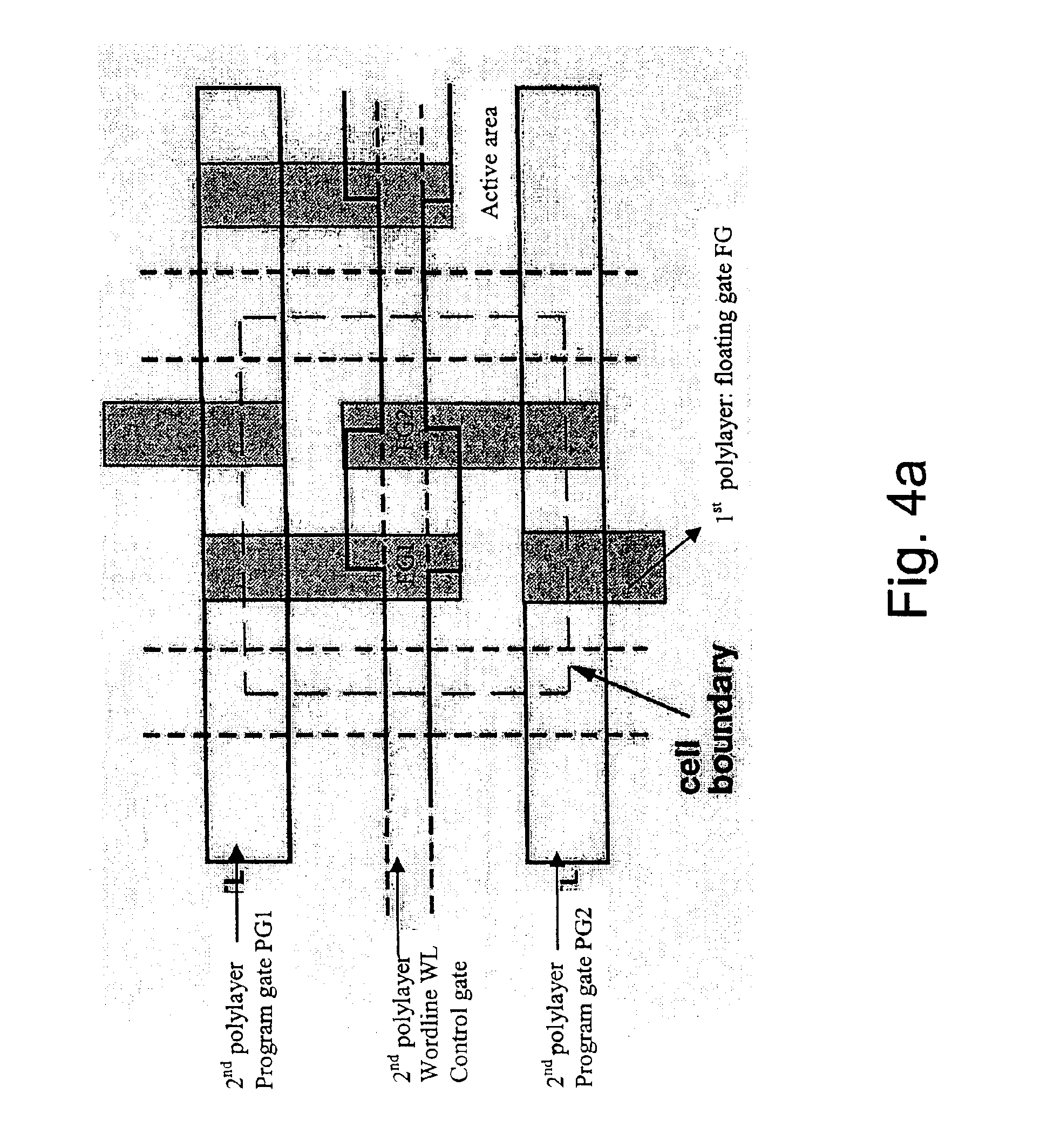
[0140]FIG. 5l shows a topview of the memory array 20 according to this third embodiment after the step of implanting the p+ field implant 11. The p+ field implant 11 electrically insulates the channel regions under the wordlines 9. The bitlines 6 are covered by either the wordline or by the planarizing dielectric 8. By removing the first polysilicon 3 in between the wordlines 9 to separate the floating gates 3, a part of the substrate 1 is exposed. This part is not covered by the planarizing dielectric 8. In this part the p+ field implant 11 can enter the substrate 1. Preferably the p+ implant 11 is given blanket but the substrate 1 area covered by the patterned polysilicon 3 will not be doped.

[0141]A second problem is related to the materials choice of the hardmask layers. First 4 and second 5 hardmask layer should preferably use materials other than oxide and nitride, in order to keep the process compatible if for example an ONO interpoly layer is used, which is to be deposited al...


PUM


Abstract

A memory is described having a semiconductor substrate of a first conductivity type, a first and a second junction region of a second conductivity type, whereby said first and said second junction region are part of respectively a first and a second bitline. A select gate is provided which is part of a wordline running perpendicular to said first and said second bitline.Read, write and erase functions for each cell make use of only two polysilicon layers which simplifies manufacture and each memory cell has at least two locations for storing a charge representing at least one bit.

Description

RELATED APPLICATIONS[0001]This application claims priority to, and hereby incorporates by reference in its entirety, now abandoned U.S. provisional application No. 60 / 391,565, filed Jun. 24, 2002, and entitled “MULTIPLE BIT NONVOLATILE MEMORY DEVICE AND METHOD FOR FABRICATING THE SAME.”[0002]This application hereby incorporates by reference the following U.S. Patents in their entirety:[0003]U.S. Pat. No. 4,794,565, issued Dec. 27, 1988, entitled “Electrically programmable memory device employing source side injection”;[0004]U.S. Pat. No. 5,278,439, issued Jan. 11, 1994, entitled “Self-aligned dual-bit split gate (DSG) flash eeprom cell”;[0005]U.S. Pat. No. 5,280,446, issued Jan. 18, 1994, entitled “Flash eprom memory circuit having source side programming”;[0006]U.S. Pat. No. 5,284,784, issued Feb. 8, 1994, entitled “Buried bit-line source-side injection flash memory cell”;[0007]U.S. Pat. No. 5,338,952, issued Aug. 16, 1994, entitled “Non-volatile memory”;[0008]U.S. Pat. No. 5,394,3...

Claims


Application Information

Patent Timeline
Patent Type & Authority Patents(United States)
IPC IPC(8): H01L21/02H01L27/115H01L21/28H01L29/66H01L29/788H01L29/792G11C16/04
CPCH01L21/2815H01L29/7923H01L27/11502H01L29/7887H01L21/28273G11C16/0458H01L29/40114H10B53/00
Inventor VAN HOUDT, JANHASPESLAGH, LUC
Owner INTERUNIVERSITAIR MICRO ELECTRONICS CENT (IMEC VZW)
Why Eureka
Try Eureka