Light emitting device

a technology of light-emitting devices and sealing techniques, which is applied in the direction of discharge tubes/lamp details, discharge tubes luminescnet screens, other domestic articles, etc., can solve the problems of insufficient life of elements, deterioration of elements, and development of dark spots, so as to prevent el element deterioration, simple and effective

Inactive Publication Date: 2005-08-02
SEMICON ENERGY LAB CO LTD
View PDF43 Cites 105 Cited by
  • Summary
  • Abstract
  • Description
  • Claims
  • Application Information

AI Technical Summary

Benefits of technology

[0022]In consideration of the above, an object of the present invention is to prevent EL element deterioration by providing a structure into which moisture and oxygen are not introduced, and by providing a simple and effective method for adding the absorption agent for absorbing moisture and oxygen, in the sealing of EL elements.
[0023]To solve the above problems, according to the present invention, improvements are made with respect to a material having an absorption property which is added, when performing enclosing of El element formed on a substrate, to the inside of the enclosed structure, and a method of adding the absorption material. Absorption films can thus be easily formed on EL elements, and in addition, EL element deterioration due to oxygen and moisture is prevented.

Problems solved by technology

Among EL elements, those using fluorescent organic compounds in their EL layers are referred to as organic EL elements, and the biggest problem in putting them to practical use is that the lifetime of the elements is insufficient.
Further, element deterioration appears as a widening of non-light emitting regions (dark spots) accompanying long light emission time, and the major cause of this deterioration is due to cathode peeling.
However, the development of dark spots has been observed even on sealing substrates.
In other words, matter adsorbed on the surface and matter emitted from the resin used in sealing exists even if the purity of the gas to be introduced is high, and therefore it is difficult to completely eliminate substances such as oxygen and moisture.
Further, since absorption agents are generally introduced by hand, the operation under an inert gas atmosphere may become more difficult.
Further, in a case where it is intended to provide a wrapped absorption agent, the wrapping itself requires much work.
There are also cases in which introduction of the absorption agent is performed within the atmosphere due to the complexities of working under an inert gas atmosphere.
However, in this case, obviously the problem with oxygen and moisture being contained within the space 1609 cannot be avoided.

Method used


Image

  • Light emitting device
  • Light emitting device
  • Light emitting device

Examples


embodiment 1

[Embodiment 1]

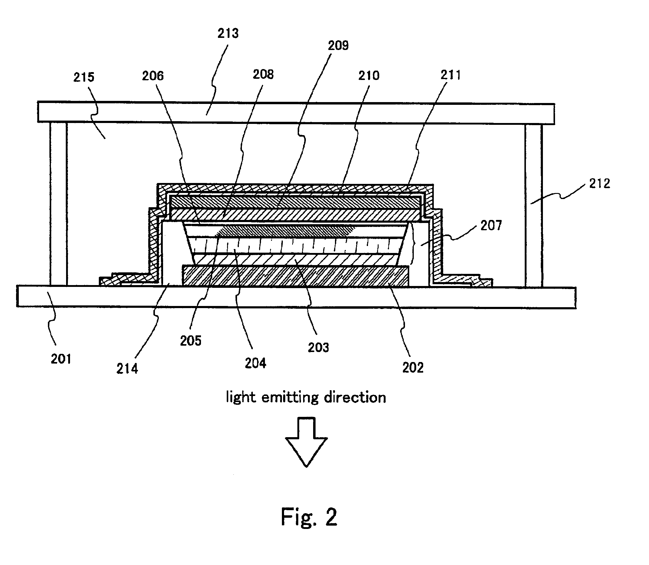
[0066]A schematic diagram of an element structure of an EL element used in implementing the present invention is shown in FIG. 2. Reference numeral 201 denotes a substrate in FIG. 2, and light transmitting materials such as glass and quartz can be used for the substrate 201. Further, reference numeral 202 denotes an anode. The anode 202 is formed by ITO, an alloy of tin oxide and indium oxide, but chemical compounds in which from 2 to 20% of zinc oxide (ZnO) is mixed into indium oxide, and chemical compounds made from zinc oxide and calcium oxide may also be used. Furthermore, edge portions of the anode 202 are covered by an insulating film 214 made from an insulating material.

[0067]An EL layer 207 is formed next having a lamination structure made from a hole injecting layer 203, a hole transporting layer 204, a light emitting layer 205, and a buffer layer 206. Specifically, copper phthalocyanine (Cu-Pc) and PEDOT, which is a polythiophene derivative, can be used in fo...

embodiment 2

[Embodiment 2]

[0090]Next, the case of using the present invention to the light-emitting device of an active matrix type is explained in this embodiment. Here, a method of simultaneously manufacturing TFTs (n-channel TFT and p-channel TFT) in a pixel portion and a driver circuit provided in the periphery of the pixel portion on the same substrate and also manufacturing an EL element is described in detail with reference to FIG. 4A to FIG. 7.

[0091]First, in this embodiment, a substrate 300 is used, which is made of glass such as barium borosilicate glass or alumino borosilicate glass, typified by #7059 glass or #1737 glass of Corning Inc. There is no limitation on the substrate 300 as long as a substrate having a light transmitting property is used, and a quartz substrate may also be used. In addition, a plastic substrate having heat resistance to a treatment temperature of this embodiment may also be used.

[0092]Then, a base film 301 formed of an insulating film such as a silicon oxid...

embodiment 3

[Embodiment 3]

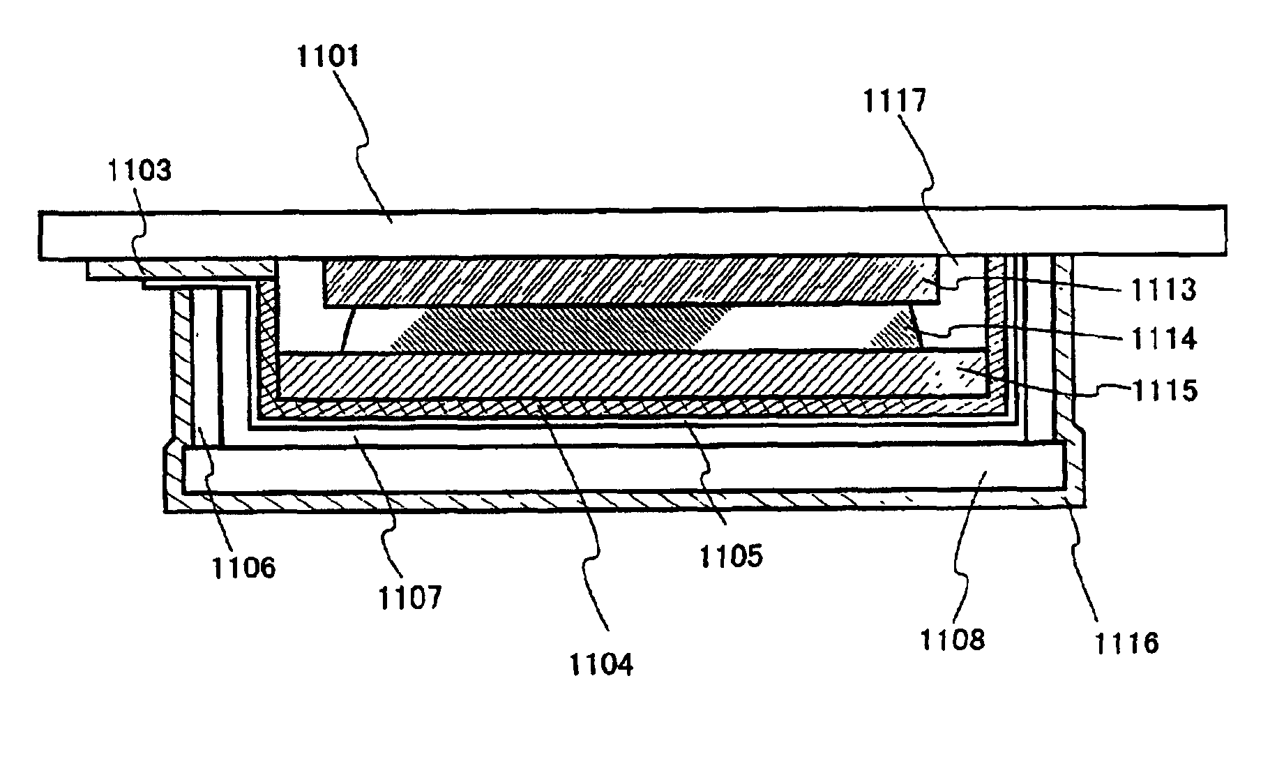
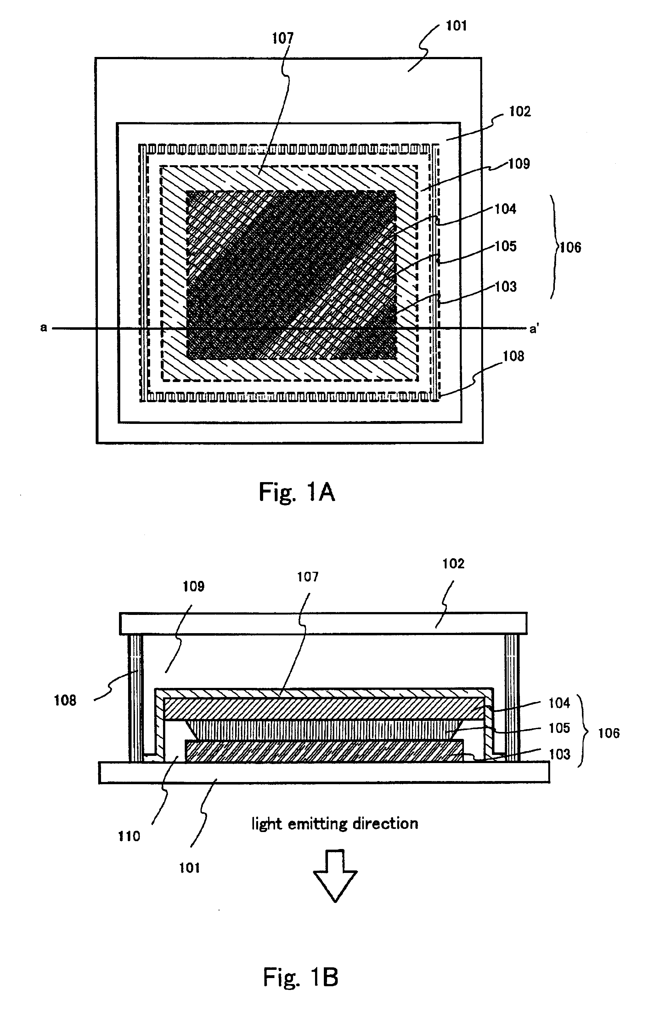
[0160]A case of using the present invention in a passive matrix (simple matrix) light emitting device is explained in this embodiment. FIG. 9 is used in the explanation. Reference numeral 1001 denotes a substrate made from glass in FIG. 9, and reference numeral 1002 denotes an anode made from a transparent conductive film. A chemical compound of indium oxide and zinc oxide is formed by sputtering as an anode 1002 in embodiment 3. Note that, although not shown in FIG. 9, a plurality of the anodes 1002 are arranged in a direction parallel to the page. In addition, banks 1003 are formed so as to be buried between the anodes 1002.

[0161]Cathodes 1006 arranged in a stripe shape are formed in a vertical direction to the page.

[0162]EL layers 1004a to 1004c composed of EL materials are formed next by evaporation, as shown by embodiment 1. Note that the EL layer 1004a is a red color light emitting EL layer, the EL layer 1004b is a green color light emitting layer, and the EL lay...


PUM


Abstract

A technique for sealing an EL panel of a light emitting device is provided. By preparing a absorption metal as a film on EL elements on the inside of an enclosed space, it becomes easy to made the interior of the space possess a absorption function, and further, an enclosure structure can be fabricated without the penetration of oxygen and moisture into the space because the absorption film is formed in succession after formation of the EL elements, according to the present invention.

Description

BACKGROUND OF THE INVENTION[0001]1. Field of the Invention[0002]The present invention relates to a device (hereinafter referred to as a light emitting device) formed by building an EL (electroluminescence) element on a substrate. In particular, the present invention relates to a sealing technique for an EL panel of a light emitting device in which EL elements formed on a substrate are sealed. Note that a module in which an FPC is connected to an EL panel, and an IC (integrated circuit) is directly mounted through the FPC, is referred to as a light emitting device within this specification.[0003]2. Description of the Related Art[0004]Research into light emitting devices having EL elements as light emitting elements has been active in recent years, and in particular, light emitting devices using organic materials as EL materials have received a lot of attention. These types of light emitting devices are referred to as organic EL displays (OELDs) or organic light emitting diodes (OLEDs...

Claims


Application Information

Patent Timeline
Patent Type & Authority Patents(United States)
IPC IPC(8): H01L51/52H01L51/50H05B33/04
CPCH01L51/5237H05B33/04Y10S428/917H10K50/846H10K50/844
Inventor OGURA, KEIITITAKAHASHI, MASAHIRO
Owner SEMICON ENERGY LAB CO LTD
Why Eureka
Try Eureka