Method for depositing a nanolaminate film by atomic layer deposition

a nanolaminate film and atomic layer deposition technology, applied in chemical vapor deposition coatings, coatings, transistors, etc., can solve the problems of inability to use gate dielectrics in fet devices, inability to find suitable replacements, and inability to deposit thin silicon dioxide interfacial layers, etc., to achieve the effect of reducing water conten

Inactive Publication Date: 2005-08-16
SHARP LAB OF AMERICA INC
View PDF7 Cites 495 Cited by
  • Summary
  • Abstract
  • Description
  • Claims
  • Application Information

AI Technical Summary

Benefits of technology

[0032]By eliminating the oxidizer steps, the present invention significantly simplifies the deposition method. The process time and the system delivery complexity are almost cut in half.
[0033]Furthermore, the elimination of separate oxidizing steps allows better control of the metal oxide compositions and therefore improves the quality of the nanolaminate films. The extra oxidizing steps of the prior art process can make the metal oxide to be oxygen-rich because of the abundance of oxygen, especially in conjunction with a nitrate precursor.
[0036]The main objective of the present invention is the use of metal nitrate-containing precursor to act as an oxidizer to control the oxygen amount introduced into the process chamber and to simplify the process flow. Therefore it is within the scope of the present invention to only retain at least one nitrate (NO3) ligand in the metal nitrate-containing precursors. Some, but not all, of the NO3 ligands can be replaced with a substituent R without affecting the effectiveness of the method. The reduction of NO3 ligands in the metal nitrate-containing precursors can also offer a control mechanism to control the oxygen amount introduced into the process chamber to adjust the property of the resulting nanolaminate films. The substituted precursors can offer tailored properties of the precursors such as volatility, and thermal stability.

Problems solved by technology

Silicon dioxide films of less than 1.5 nm generally cannot be used as a gate dielectric in FET devices mainly because of the excessive power consumption due to the high leakage from the direct tunneling currents.
There are also other fabrication and reliability concerns for such a very thin silicon dioxide film such as boron penetration, and charge injection damage.
Many high dielectric constant dielectric materials (high k dielectric) have been investigated as possible replacements for silicon dioxide but a suitable replacement has still not been found because of the many other stringent requirements such as low leakage current, formation of a good interface with silicon substrate, low thermal budget for the fabrication process, and device high channel mobility.
The presence of the thin silicon dioxide interfacial layer is not desirable because it is then very difficult to achieve a silicon dioxide equivalent thickness of 1nm.
However, the deposited hafnium oxide films still suffer from various problems.
One problem is its low crystallization temperature, resulting in a much lower thermal budget for the fabrication process of the semiconductor devices.
Another problem is that the quality of the interface of hafnium oxide and silicon substrate is relatively poor with respect to silicon dioxide / silicon interface and that results in low channel mobility when integrated into semiconductor device structures.
CVD typically requires high temperature, in the order of 400 to 800° C. CVD at lower temperature tends to produce low quality films in terms of uniformity and impurities.
The uniformity of CVD film is also a function of process conditions, and in general is not very good at very thin films.
Thus many useful CVD precursors are not viable as ALD precursors and vice versa.
However; our research has shown that hafnium oxide deposited via hafnium nitrate together with an oxidizing agent has a dielectric constant lower than expected, probably due to the oxygen-rich nature of the hafnium oxide film.

Method used


Image

  • Method for depositing a nanolaminate film by atomic layer deposition
  • Method for depositing a nanolaminate film by atomic layer deposition
  • Method for depositing a nanolaminate film by atomic layer deposition

Examples


Embodiment Construction

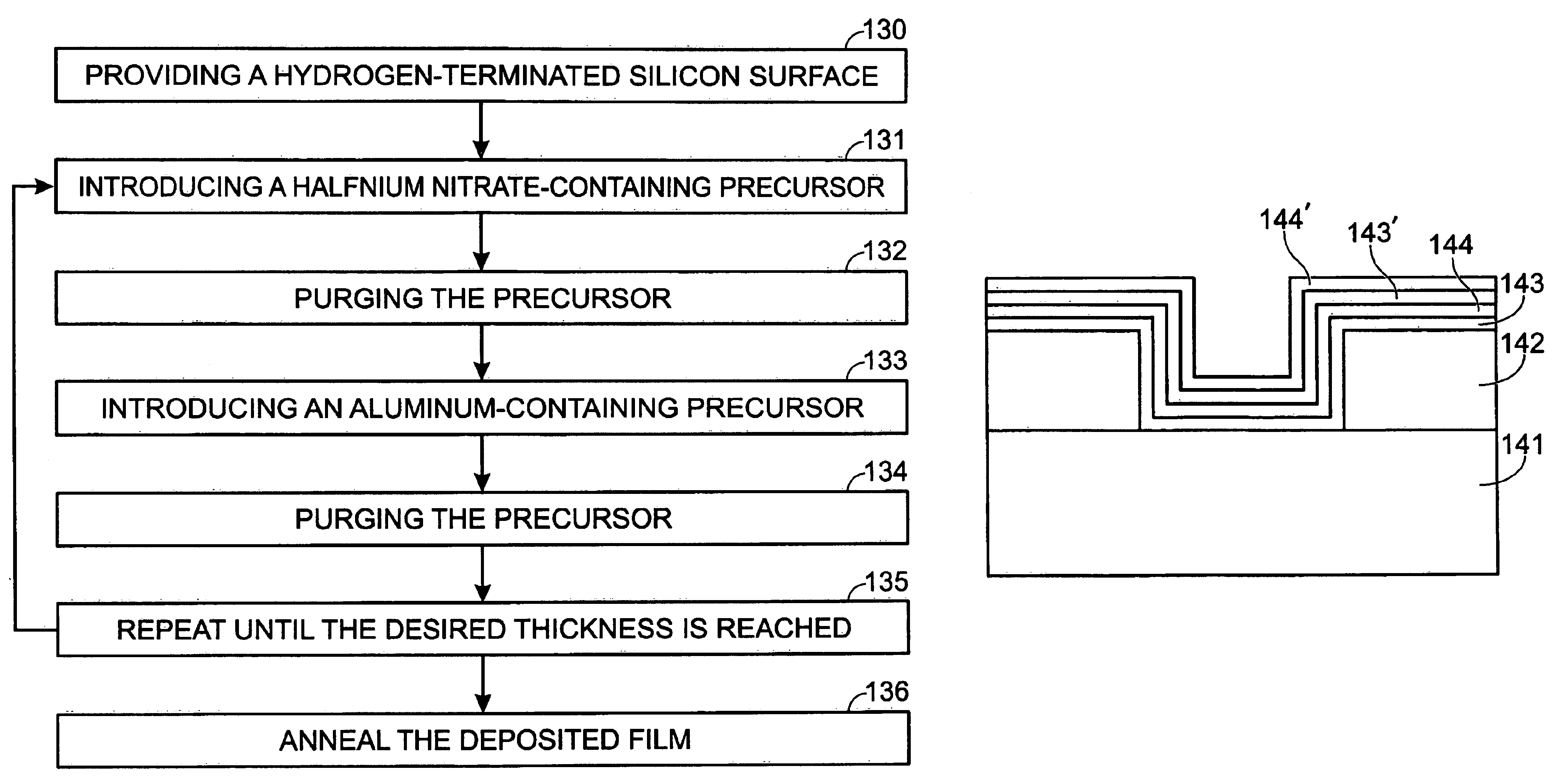
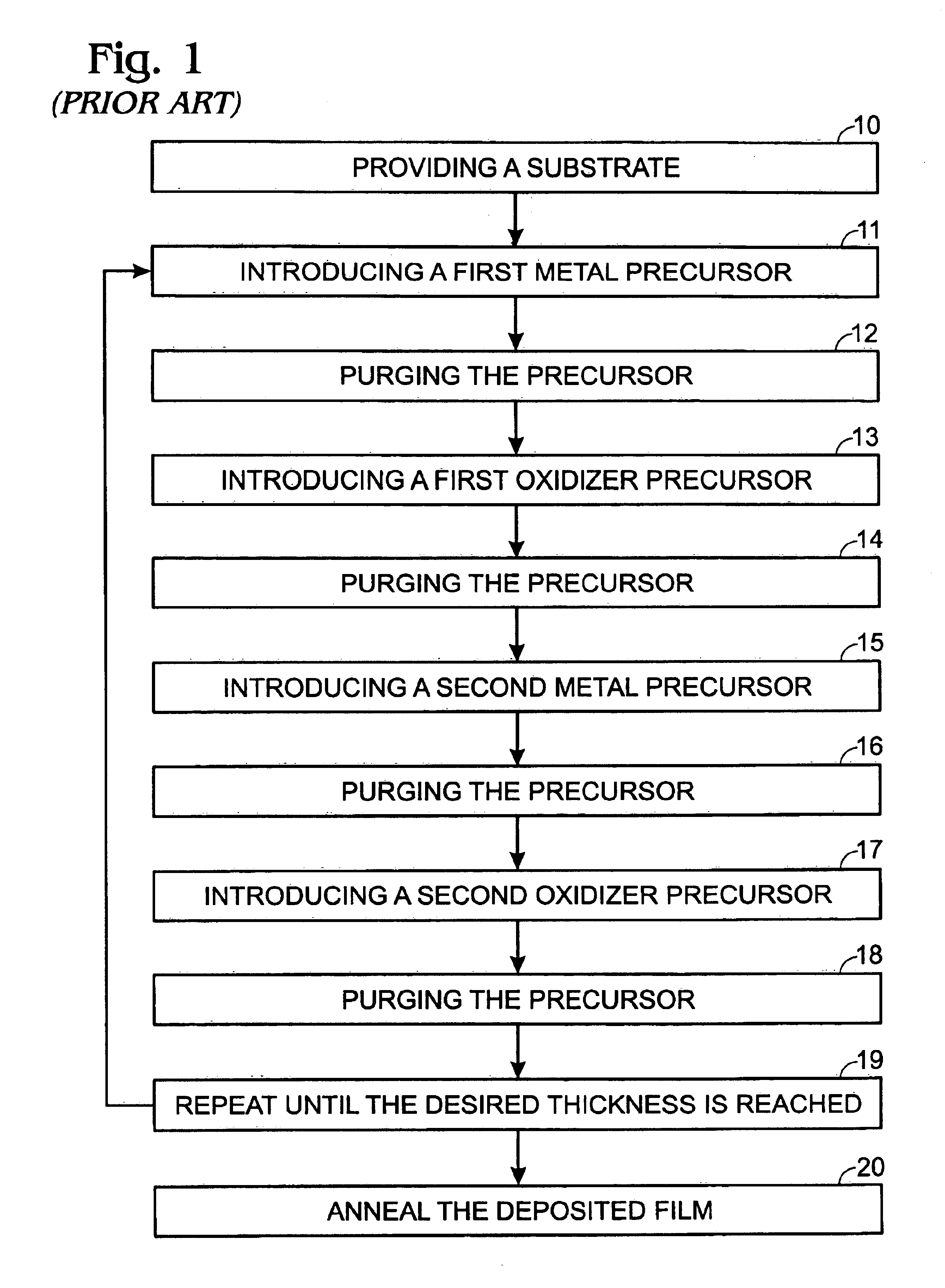
[0053]FIG. 1 shows a flowchart of a prior art process showing the steps of depositing an oxide nanolaminate thin film. Step 10 provides a substrate within a process chamber. The substrate and the chamber are conditioned for the deposition process such as the growing of an oxide interface layer (step 10a). Steps 11 to 14 provide the first metal oxide of the two-oxide nanolaminate thin film. Step 11 provides a first metal precursor for an adsorption of the precursor onto the substrate such as hafnium chloride (HfCl4). Step 12 provides a purging step to remove the precursor from the process chamber with an inactive gas such as nitrogen. Step 13 provides a first oxidizer such as water, alcohol, oxygen, or ozone to the process chamber. The oxidizer reacts with the adsorbed first metal precursor to form a first metal oxide such as hafnium oxide. Step 14 provides a purging step with nitrogen to remove the oxidizer and any by-products. Then the second metal oxide of the two-oxide nanolamina...


PUM

PropertyMeasurementUnit
dielectric constantaaaaaaaaaa
thicknessaaaaaaaaaa
thicknessaaaaaaaaaa

Abstract

An atomic layer deposition method to deposit an oxide nanolaminate thin film is provided. The method employs a nitrate ligand in a first precursor as an oxidizer for a second precursor to form the oxide nanolaminates. Using a hafnium nitrate precursor and an aluminum precursor, the method is well suited for the deposition of a high k hafnium oxide / aluminum oxide nanolaminate dielectric for gate dielectric or capacitor dielectric applications on a hydrogen-terminated silicon surface.

Description

CROSS-REFERENCE TO RELATED PATENT APPLICATION[0001]The present application is related to application Ser. No. 10 / 376,774, entitled “Atomic layer of deposition of oxide film,” invented by the inventors of the present invention and filed Feb. 27, 2003.FIELD OF THE INVENTION[0002]The present invention relates to an atomic layer deposition (ALD) method to deposit a metal oxide nanolaminate film by using a metal nitrate-containing precursor as an oxidizing agent for another metal-containing precursor. The invention may be used in numerous applications, including electro-optic structures, optical coating, and passivation coating for metallurgical and biomedical applications. Particularly, the present invention relates to integrated circuit fabrication, and specifically to a gate dielectric for a semiconductor transistor and a capacitor dielectric for a memory circuit.BACKGROUND OF THE INVENTION[0003]Dielectric materials in semiconductor devices in integrated circuits appear as gate dielec...

Claims


Application Information

Patent Timeline
Patent Type & Authority Patents(United States)
IPC IPC(8): C23C16/56C23C16/40H01L21/02H01L21/28H01L21/336H01L21/314H01L29/51H01L29/40C23C16/44H01L29/49H01L21/316H01L21/205C23C16/455H01L21/8242H01L27/108
CPCC23C16/40H01L29/66583C23C16/45531C23C16/56H01L21/28185H01L21/28194H01L21/28202H01L21/3142H01L29/513C23C16/45529H01L21/31616H01L21/31645H01L29/4908H01L29/517H01L29/518H01L21/02205H01L21/02181H01L21/02178H01L21/0228H01L21/022
Inventor CONLEY, JR., JOHN F.ONO, YOSHISOLANKI, RAJENDRA
Owner SHARP LAB OF AMERICA INC
Why Eureka
Try Eureka