Scalable high performance antifuse structure and process

a high-performance, anti-fuse technology, applied in the direction of electrical equipment, semiconductor devices, semiconductor/solid-state device details, etc., can solve the problems of high voltage, high voltage, complex circuits, etc., and achieve low capacitance, reduced programming voltage, and high performance

Inactive Publication Date: 2005-09-13
MICRON TECH INC
View PDF43 Cites 14 Cited by
  • Summary
  • Abstract
  • Description
  • Claims
  • Application Information

AI Technical Summary

Benefits of technology

[0010]The above mentioned problems are addressed by the present subject matter and will be understood by reading and studying the following specification. The present subject matter provides a scalable high-performance antifuse structure and process. The antifuse structure has a very low effective dielectric constant (keff) that includes a very low dielectric constant material and air, i.e. a controlled amount of porosity or void, to achieve a low capacitance. As such, the RC component attributable to the antifuse structure is low. Furthermore, the antifuse structure includes injector Silicon Rich Insulator (SRI), such as Silicon Rich Nitride (SRN), to provide a uniform breakdown of the antifuse dielectric and a significantly reduced programming voltage such that the programming voltage is capable of being scaled with Vdd. As such, the present subject matter is capable of being used in high performance and low power applications.

Problems solved by technology

It often is not cost effective to create separate fabrication lines, with different masks and such, for each small change for various applications.
This high voltage requires complex circuits for generating the high programming voltage on-chip as well as complex processing for routing such high voltages across the chip in an integrated circuit that is otherwise scaled for low voltage.
One particular problem confronting the semiconductor industry is the challenge of reducing antifuse capacitance to enhance programming performance while lowering the programming voltage for Field Programmable Gate Arrays (FPGAs) and Alterable Logic Devices (ALDs).
This capacitive component of antifuses contributes significantly to the signal transmission delay of FPGA or ALD devices.
Thinner oxide provides each antifuse with a higher capacitance, which results in a slower device performance.
The increased capacitive components of the antifuses increase RC components, which increases logic delays and adversely affects the performance of the FPGA or ALD devices.
One limitation of these films is the thickness and scalability of the SiO2 layer, and the associated parasitic capacitance.
The oxide thickness does not scale proportionately with the scaling of the technology and power supply generations because the antifuse device leakage in the open state is not acceptable.

Method used


Image

  • Scalable high performance antifuse structure and process
  • Scalable high performance antifuse structure and process
  • Scalable high performance antifuse structure and process

Examples


Embodiment Construction

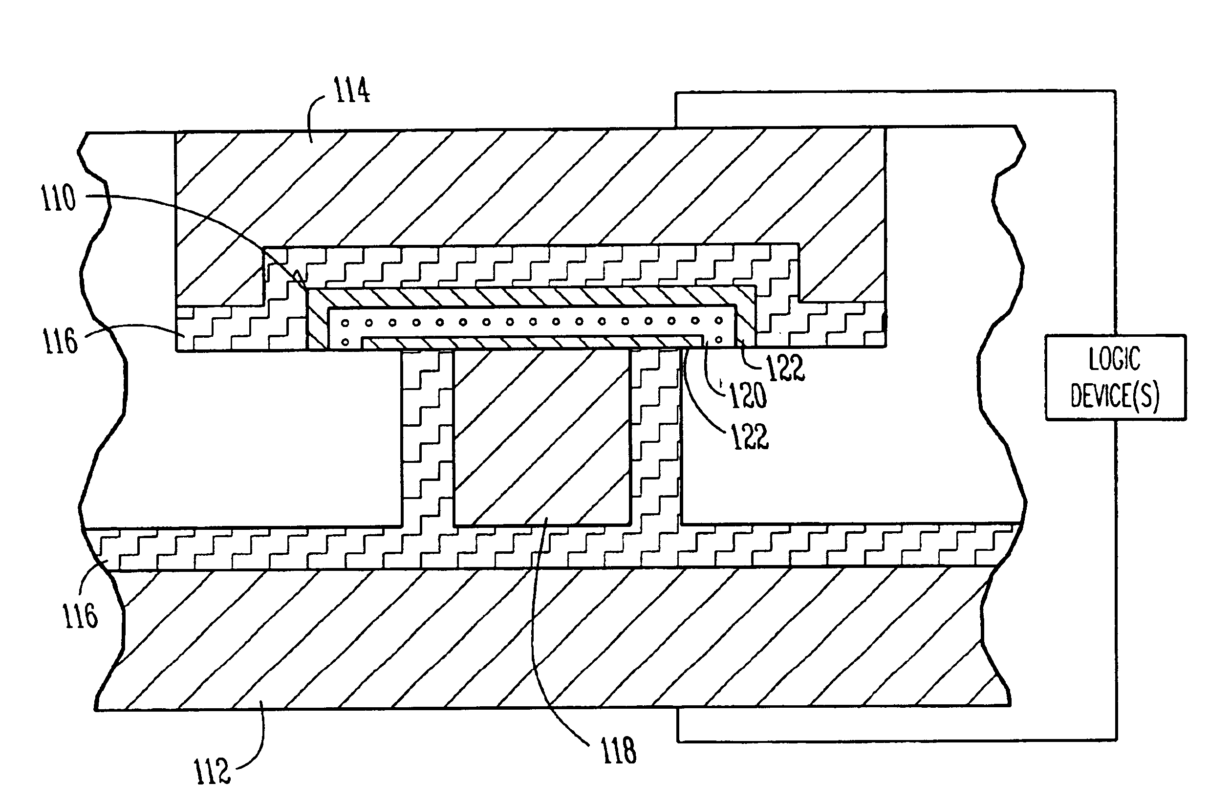
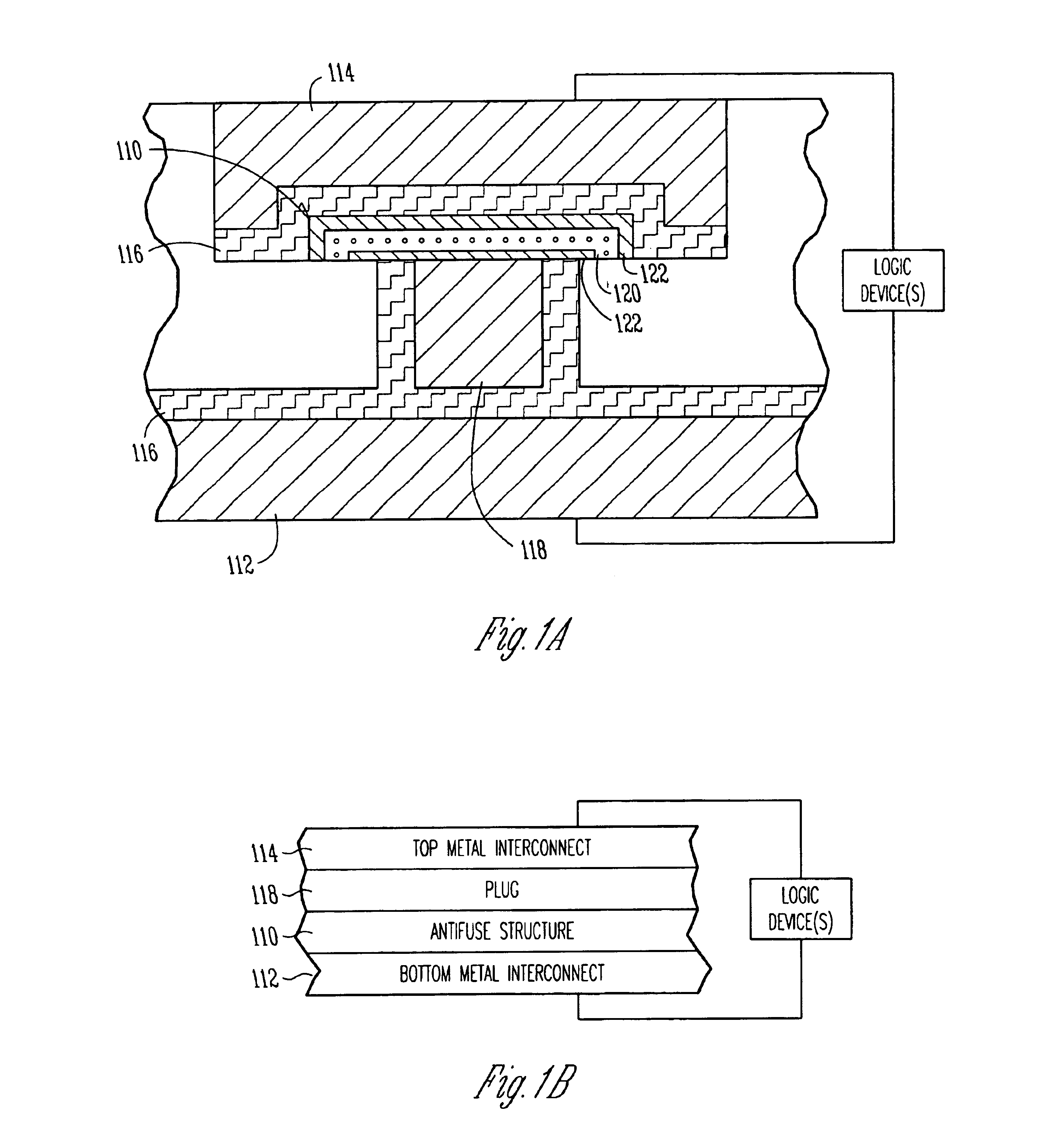
[0033]The following detailed description of the invention refers to the accompanying drawings which show, by way of illustration, specific aspects and embodiments in which the invention may be practiced. In the drawings, like numerals describe substantially similar components throughout the several views. These embodiments are described in sufficient detail to enable those skilled in the art to practice the invention. Other embodiments may be utilized and structural, logical, and electrical changes may be made without departing from the scope of the present invention. The following detailed description is, therefore, not to be taken in a limiting sense, and the scope of the present invention is defined only by the appended claims, along with the full scope of equivalents to which such claims are entitled.

[0034]The present subject matter provides a scalable high-performance antifuse structure and process by providing a low-k dielectric medium with a controlled porosity as the core el...


PUM

PropertyMeasurementUnit
thickaaaaaaaaaa
thickaaaaaaaaaa
dielectric constantaaaaaaaaaa

Abstract

Systems and methods are provided for a scalable high-performance antifuse structure and process that has a low RC component, a uniform dielectric breakdown, and a very low, effective dielectric constant (keff) such that a programming pulse voltage is scalable with Vdd. One aspect of the present subject matter is an antifuse device that is positioned or coupled between a first metal level and a second metal level. One embodiment of the antifuse device includes a porous antifuse dielectric layer, and at least one injector Silicon-Rich-Insulator (SRI) layer in contact with the porous antifuse dielectric layer. In one embodiment, the porous antifuse dielectric layer includes SiO2 formed with air-filled voids. In one embodiment, the at least one injector SRI layer includes two injector Silicon-Rich-Nitride layers that sandwich the porous antifuse dielectric layer. Other aspects are provided herein.

Description

CROSS REFERENCE TO RELATED APPLICATIONS[0001]This application is related to the following co-pending, commonly assigned U.S. patent applications which are herein incorporated by reference in its entirety: “Low K Interconnect Dielectric Using Surface Transformation,” Ser. No. 10 / 106,915, filed on Mar. 25, 2002.TECHNICAL FIELD OF THE INVENTION[0002]This invention relates generally to integrated circuits and, more particularly, to integrated circuit antifuses.BACKGROUND OF THE INVENTION[0003]Integrated semiconductor circuits or devices are designed and used for widely differing applications. It often is not cost effective to create separate fabrication lines, with different masks and such, for each small change for various applications. As such, the device is personalized to meet various needs by opening and closing links using various techniques.[0004]One technique for opening a previously closed link involves fuses. The appropriate fuses are blown by a laser or other means to persona...

Claims


Application Information

Patent Timeline
Patent Type & Authority Patents(United States)
IPC IPC(8): H01L23/525H01L23/52
CPCH01L23/5252H01L2924/0002H01L2924/00
Inventor BHATTACHARYYA, ARUPGEUSIC, JOSEPH E.
Owner MICRON TECH INC
Why Eureka
Try Eureka