Amorphous diamond materials and associated methods for the use and manufacture thereof

a technology of diamond materials and diamonds, applied in the manufacture of discharge tubes/lamps, discharge tube main electrodes, electrode systems, etc., can solve the problems of limiting the potential and limiting the use of field emission devices. , to achieve the effect of improving the collection of energy

Inactive Publication Date: 2005-09-27
SUNG CHIEN MIN
View PDF35 Cites 11 Cited by
  • Summary
  • Abstract
  • Description
  • Claims
  • Application Information

AI Technical Summary

Benefits of technology

[0011]In one alternative embodiment, the intermediate member can be formed of a thermally insulating material having a plurality of apertures extending therethrough. The plurality of apertures can contain a conductive metal. Various configurations of apertures and conductive materials allow for tailoring of the overall thermal and electrical conductivity of the intermediate member.
[0012]In another detailed aspect, an energy collector can be coupled to the cathode opposite the amorphous diamond material to enhance collection of energy to be directed toward the amorphous diamond layer. As an example, the energy collector can be a layer of carbon black, a rough surface having asperities in the nanometer or micron range or any other energy collecting material.

Problems solved by technology

Although basically successful in many applications, thermionic devices have been less successful than field emission devices, as field emission devices generally achieve a higher current output.
Despite this key advantage, most field emission devices suffer from a variety of other shortcomings that limit their potential uses, including materials limitations, versatility limitations, cost effectiveness, lifespan limitations, and efficiency limitations, among others.
While such attempts have achieved moderate success, a number of limitations on performance, efficiency, and cost, still exist.
Therefore, the possible applications for field emitters remain limited to small scale, low current output applications.

Method used


Image

  • Amorphous diamond materials and associated methods for the use and manufacture thereof
  • Amorphous diamond materials and associated methods for the use and manufacture thereof
  • Amorphous diamond materials and associated methods for the use and manufacture thereof

Examples


example 1

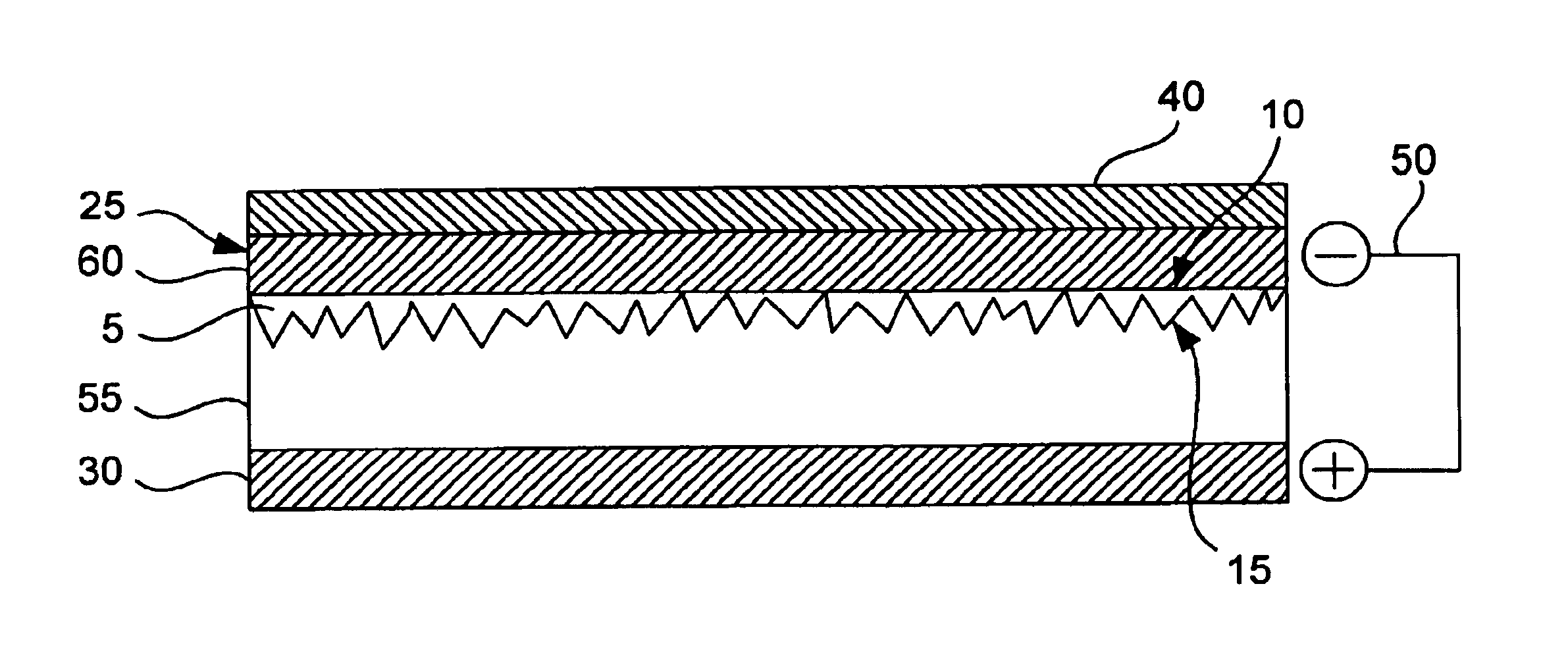
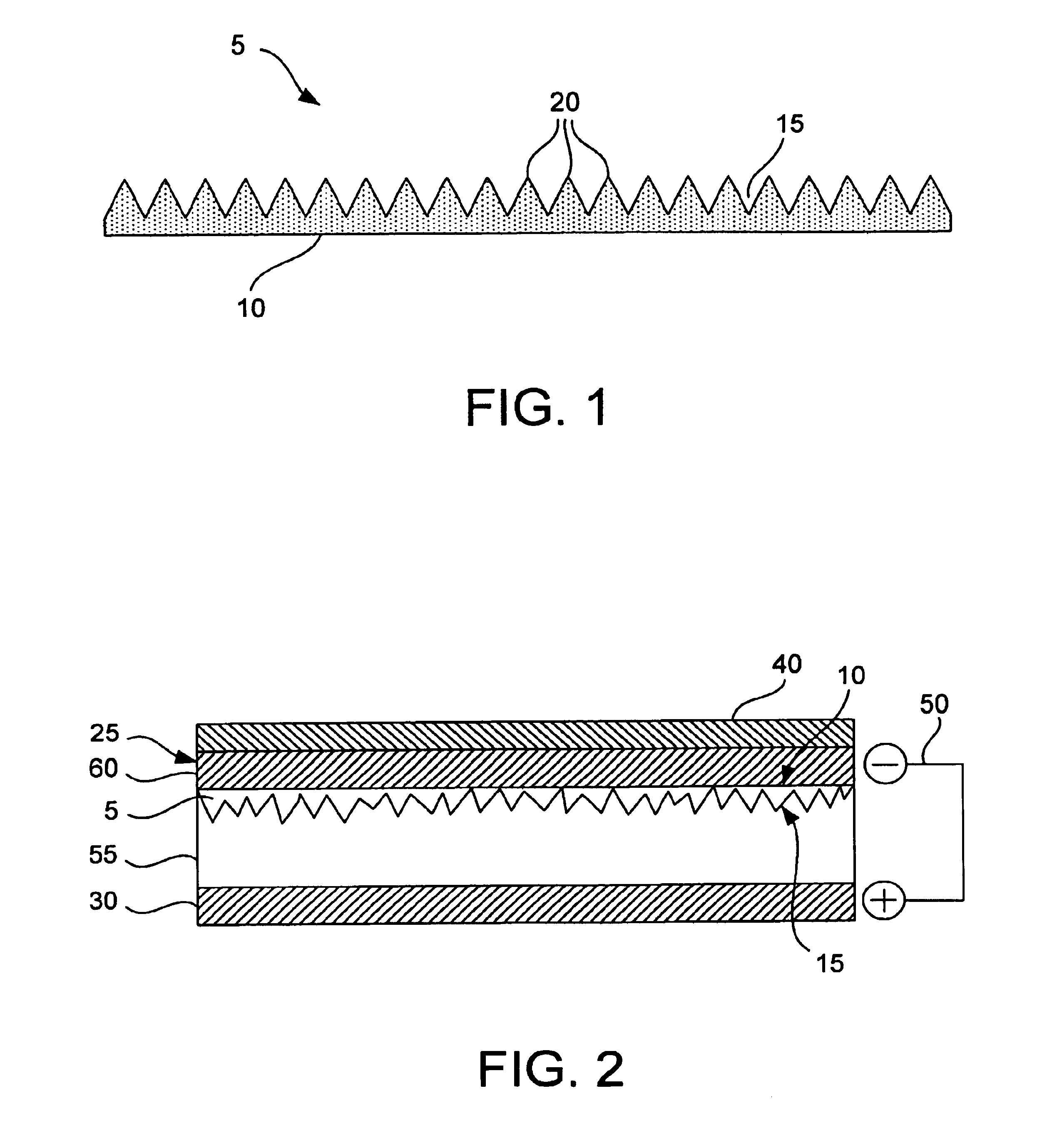
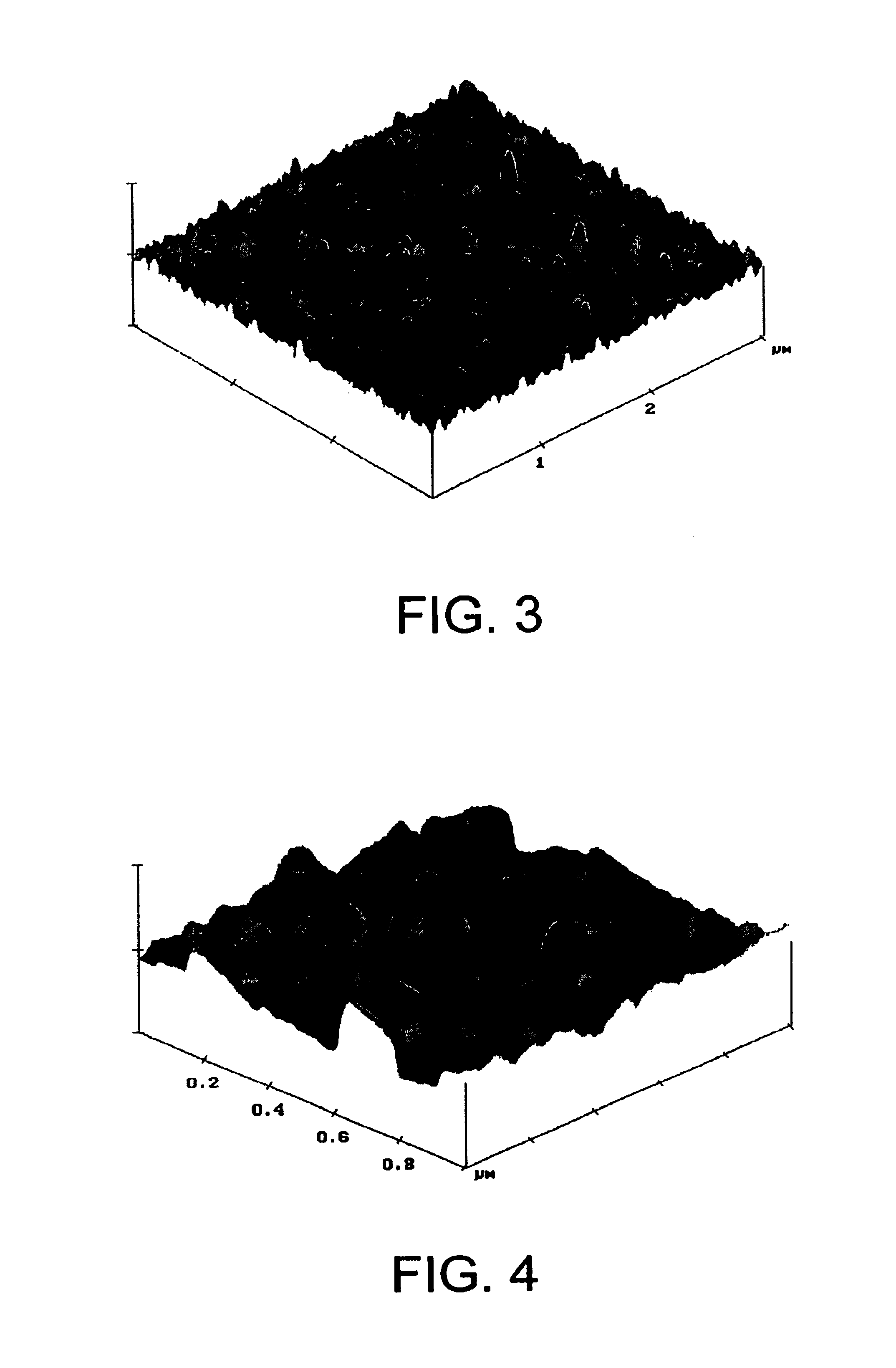
[0075]An amorphous diamond material was made as shown in FIG. 3, using cathodic arc deposition. Notably, the asperity of the emission surface has a height of about 200 nanometers, and a peak density of about 1 billion peaks per square centimeter. In the fabrication of such material, first, a silicon substrate of N-type wafer with (200) orientation was etched by Ar ions for about 20 minutes. Next, the etched silicon wafer was coated with amorphous diamond using a Tetrabond® coating system made by Multi-Arc, Rockaway, N.J. The graphite electrode of the coating system was vaporized to form an electrical arc with a current of 80 amps, and the arc was drive by a negative bias of 20 volts toward the silicon substrate, and deposited thereon. The resulting amorphous diamond material was removed from the coating system and observed under an atomic force microscope, as shown in FIGS. 3 and 4.

[0076]The amorphous diamond material was then coupled to an electrode to form a cathode, and an electr...

example 2

[0077]A 10 micron layer of copper can be deposited on a substrate using sputtering. Onto the copper was deposited 2 microns of samarium by sputtering onto the copper surface under vacuum. Of course, care should be taken so as to not expose the beryllium to oxidizing atmosphere (e.g. the entire process can be performed under a vacuum). A layer of amorphous diamond material can then be deposited using the cathodic arc technique as in Example 1 resulting in a thickness of about 0.5 microns. Onto the growth surface of the amorphous diamond a layer of magnesium can be deposited by sputtering, resulting in a thickness of about 10 microns. Finally a 10 microns thick layer of copper was deposited by sputtering to form the anode.

example 3

[0078]A 10 micron layer of copper can be deposited on a substrate using sputtering. Onto the copper was deposited 2 microns of cesium by sputtering onto the copper surface under vacuum. Of course, care should be taken so as to not expose the cesium to oxidizing atmosphere (e.g. the entire process can be performed under a vacuum). A layer of amorphous diamond material can then be deposited using the cathodic arc technique as in Example 1 resulting in a thickness of about 65 nm. Onto the growth surface of the amorphous diamond a layer of molybdenum can be deposited by sputtering, resulting in a thickness of about 16 nm. Additionally, a 20 nm thick layer of In—Sn oxide was deposited by sputtering to form the anode. Finally, a 10 micron layer of copper was deposited on the In—Sn layer by sputtering. The cross-sectional composition of the assembled layers is shown in part by FIG. 9A as deposited. The assembled layers were then heated to 400° C. in a vacuum furnace. The cross-sectional co...


PUM

PropertyMeasurementUnit
heightaaaaaaaaaa
work functionaaaaaaaaaa
thicknessaaaaaaaaaa

Abstract

An amorphous diamond electrical generator having a cathode at least partially coated with amorphous diamond material and an intermediate member coupled between the cathode and an anode. The amorphous diamond material can have at least about 90% carbon atoms with at least about 20% of the carbon atoms bonded in a distorted tetrahedral coordination. The amorphous diamond coating has an energy input surface in contact with a base member of the cathode and an electron emission surface opposite the energy input surface. The electron emission surface can have an asperity height of from about 10 to about 1,000 nanometers and is capable of emitting electrons upon input of a sufficient amount of energy. The intermediate member can be coupled to the electron emission surface of the amorphous diamond coating such that the intermediate member has a thermal conductivity of less than about 100 W / mK and a resistivity of less than about 80 μΩ-cm at 20° C. The amorphous diamond electrical generator is a thermionic emission device having improved electron emission properties.

Description

PRIORITY DATA[0001]This application is a continuation-in-part of U.S. patent application Ser. No. 10 / 094,425, filed on Mar. 8, 2002, now U.S. Pat. No. 6,806,624 which is incorporated herein by reference.FIELD OF THE INVENTION[0002]The present invention relates generally to devices and methods for generating electrons from diamond-like carbon material. Accordingly, the present application involves the fields of physics, chemistry, electricity, and material science.BACKGROUND OF THE INVENTION[0003]Thermionic and field emission devices are well known and used in a variety of applications. Field emission devices such as cathode ray tubes and field emission displays are common examples of such devices. Generally, thermionic electron emission devices operate by ejecting hot electrons over a potential barrier, while field emission devices operate by causing electrons to tunnel through a barrier. Examples of specific devices include those disclosed in U.S. Pat. Nos. 6,229,083; 6,204,595; 6,...

Claims


Application Information

Patent Timeline
Patent Type & Authority Patents(United States)
IPC IPC(8): C01B31/06C01B31/00H01J1/304H01J1/13H01J1/30H01J1/14H01JH01J1/02H01J1/16H01J9/02
CPCC01B31/06H01J1/304H01J1/3048H01J9/025H01J2201/30446H01J2201/30457C01B32/26C01B32/25
Inventor SUNG, CHIEN-MIN
Owner SUNG CHIEN MIN
Why Eureka
Try Eureka