Optical semiconductor device having an epitaxial layer of III-V compound semiconductor material containing N as a group V element

a compound semiconductor material and semiconductor technology, applied in the field of optical semiconductor devices, can solve the problems of difficult formation of the electrode on the bottom surface of the sapphire substrate b>11/b>, difficult preparation of the single crystal substrate of gan, etc., and achieve the effect of minimizing the resistance at the interface between the sic substrate and the algan buffer layer

Inactive Publication Date: 2006-01-10
FUJITSU LTD
View PDF27 Cites 17 Cited by
  • Summary
  • Abstract
  • Description
  • Claims
  • Application Information

AI Technical Summary

Benefits of technology

[0092]According to the present invention, the resistance at the interf

Problems solved by technology

It should be noted that GaN has a Wurtzite structure belonging to the hexagonal crystal system, and the preparation of a single crystal substrate of GaN is difficult.
The laser diode of FIG. 1, however, has a drawback in that, due to the existence of large lattice misfit of as much as 13% or more at the heteroepitaxial interface between the c-surface of the sapphire single crystal substrate 11 and the GaN epitaxial layer 12, the epitaxial layers 15–17 forming the MQW structure 16 tend to include various crystal defects with a high concentration level.
Further, the laser diode 1 of FIG. 1 has a difficulty, contrary to the conventional edge-emission type, in that formation of the electrode on the bottom surface of the sapphire substrate 11 is difficult.
Thereby, the construction, and hence the fabrication process of the laser diode becomes inevitably complex.
In addition, the sapphire substrate used in the laser diode 1 is difficult to be cleaved, and thus, it is difficult in the laser diode 1 to form the mirror surfaces by a conventional cleaving process, contrary to the conventional edge-emission type laser di

Method used


Image

  • Optical semiconductor device having an epitaxial layer of III-V compound semiconductor material containing N as a group V element
  • Optical semiconductor device having an epitaxial layer of III-V compound semiconductor material containing N as a group V element
  • Optical semiconductor device having an epitaxial layer of III-V compound semiconductor material containing N as a group V element

Examples


first embodiment

[First Embodiment]

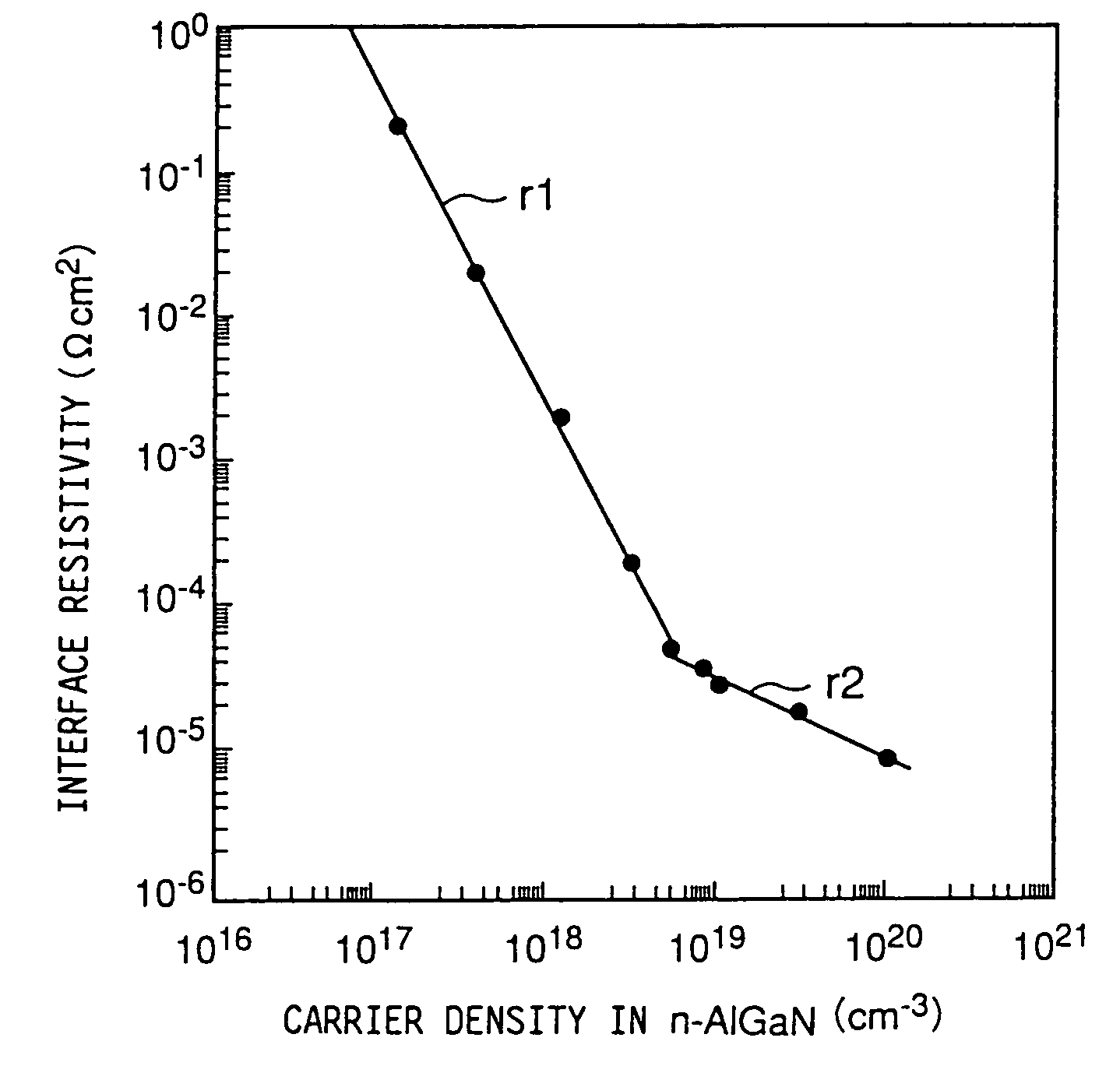
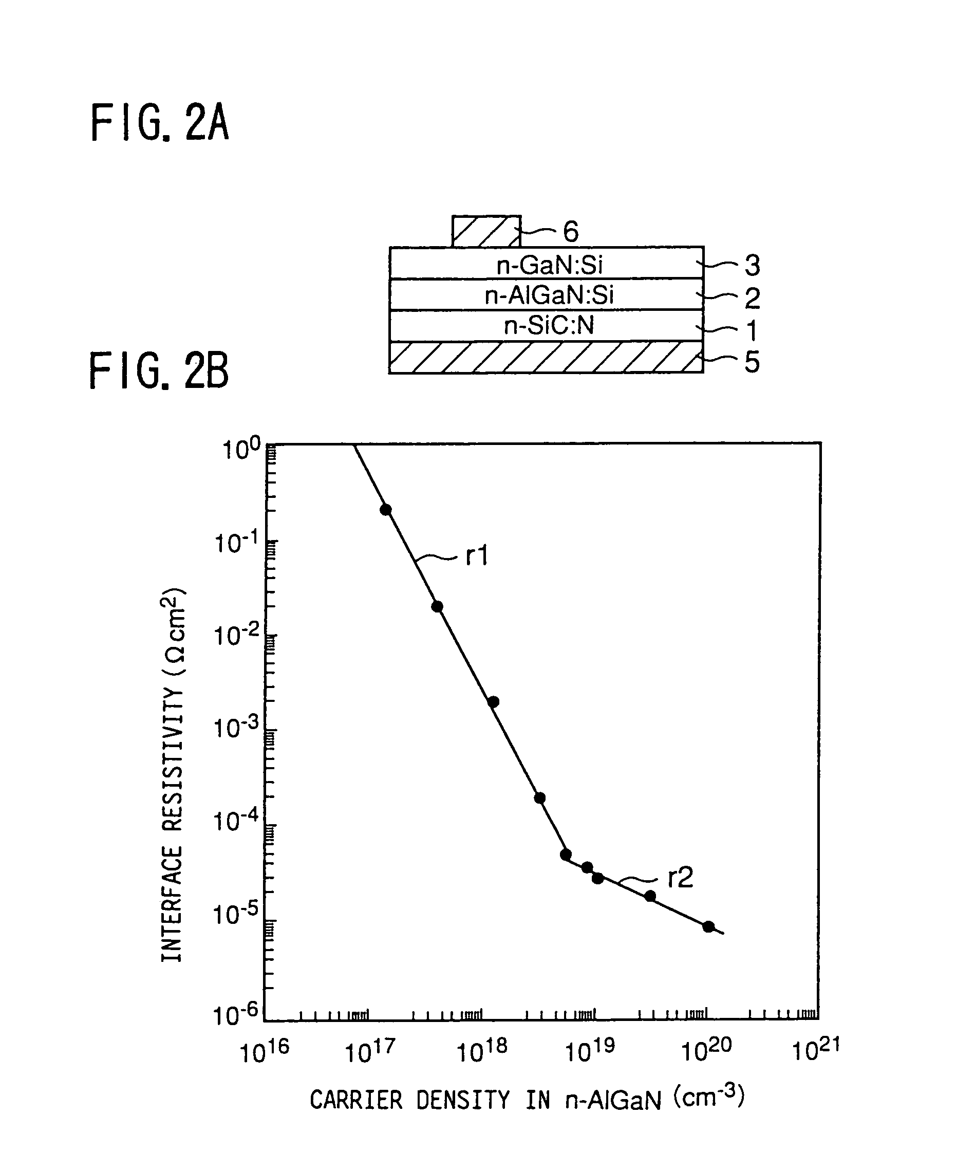
[0113]In the description hereinafter, the mixed crystal having the composition AlxGa1-xN (0

[0114]Thus, it is possible to construct a GaN-family laser diode on an n-type SiC substrate covered by an n-type AlxGa1-xN buffer layer, by depositing desired epitaxial layers of GaN or a mixed crystal of GaN. The laser diode thus formed typically oscillates at the wavelength of 420 nm ...

second embodiment

[Second Embodiment]

[0167]During the experimental investigation on the GaN-family laser diode 100 described with reference to FIGS. 6A and 6B, the inventor of the present invention has discovered a relationship shown in FIG. 7 between the threshold current and the thickness of the epitaxial layers interposed between the SiC substrate 41 and the active layer structure 40, wherein the vertical axis represents the threshold current density of the laser diode while the horizontal axis represents the total thickness of the epitaxial layers interposed between the SiC substrate 31 and the active layer structure 40.

[0168]Referring to FIG. 7, the threshold current generally decreases with increasing thickness in the epitaxial layers interposed between the substrate 31 and the active layer 40 and that the decrease occurs sharply until the total thickness of the epitaxial layers reach the value of about 1.6 μm.

[0169]While the reason of this phenomenon is not clearly understood, it is probable t...

third embodiment

[Third Embodiment]

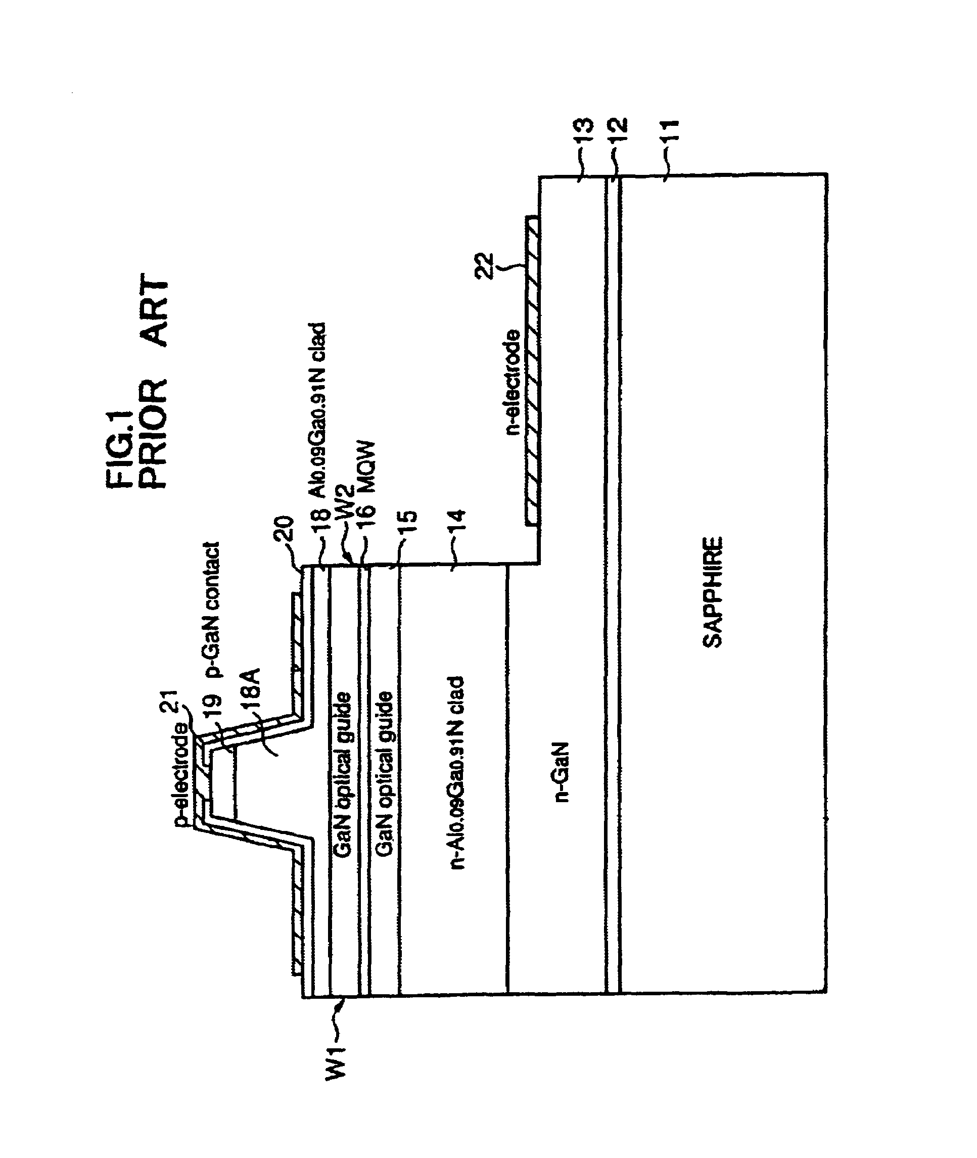
[0179]In the ridge-type laser diode 100, 200 or 210 described before, the control of transversal mode laser oscillation in the active layer structure 40 is achieved by forming a mesa structure in the upper cladding layer 53 as explained before.

[0180]In the ridge-type laser diode having such a structure, it is necessary to form the mesa structure to have a width of less than about 2 μm in order to achieve a satisfactory control of the transversal mode oscillation, while the formation of such a narrow mesa structure has been difficult. Further, the foregoing conventional ridge-type laser diode has a drawback in that the contact area between the electrode 62 and the contact layer 54 is reduced inevitably when the width of the mesa structure is thus reduced below 2 μm. It should be noted that the width of the contact window formed in the SiO2 film 61 is reduced together with the width of the mesa structure, while formation of such a very small contact window in the SiO...


PUM


Abstract

An optical semiconductor device includes an SiC substrate having an n-type conductivity, and an AlGaN buffer layer having an n-type conductivity formed on the SiC substrate with a composition represented as AlxGa1-xN, wherein the AlGaN buffer layer has a carrier density in the range between 3×10¹⁸–1×1020 cm−3, and the compositional parameter x is larger than 0 but smaller than 0.4 (0<x<0.4).

Description

BACKGROUND OF THE INVENTION[0001]The present invention generally relates to optical semiconductor devices and more particularly to a GaN-family laser diode producing blue to ultraviolet radiation and a fabrication process thereof.[0002]Laser diodes, light-emitting diodes and photodiodes are optical semiconductor devices used extensively in the field of optical telecommunication, optical information processing, recording of information, and the like.[0003]In the case of laser diode, there is a demand, particularly in the field of optical information recording, for a laser diode operable in the optical wavelength band of blue to ultraviolet radiation for increasing the recording density. It should be noted a laser diode oscillates generally in the optical wavelength band of red to infrared radiation. Further, there is a demand for a photodiode operable in such a short optical wavelength band.[0004]Conventionally, GaN, having a large bandgap, has been recognized as a promising material...

Claims


Application Information

Patent Timeline
IPC IPC(8): H01L29/06H01L21/205B82Y10/00B82Y20/00B82Y40/00H01L21/20H01S5/00H01S5/223H01S5/323H01S5/343
CPCB82Y20/00H01L21/02378H01L21/02458H01L21/02502H01L21/0254H01L21/0262H01S5/34333H01L33/32H01S5/2231H01L33/007H01S5/0421H01S5/2205H01L21/02636
Inventor KURAMATA, AKITOKUBOTA, SHINICHIHORINO, KAZUHIKOSOEJIMA, REIKO
Owner FUJITSU LTD
Why Eureka
Try Eureka