Electron emitting device, electron source and image display device and methods of manufacturing these devices

a technology image display device, which is applied in the field of electron emitting device, electron source, image display device, etc., can solve the problems of deteriorating uniformity in forming many electron-emitting devices, complicated control of each step, and unfavorable control of electron emission characteristics and reproducibility, so as to improve the production method of the present invention and improve the reproducibility of electron emission. , the effect of improving the reproducibility

Inactive Publication Date: 2006-01-31
CANON KK
View PDF86 Cites 12 Cited by
  • Summary
  • Abstract
  • Description
  • Claims
  • Application Information

AI Technical Summary

Benefits of technology

[0129]In each of the electron-emitting devices of the present invention, a space serving as an electron emission section can be formed at a predetermined position, and thus the electron emission characteristics and reproducibility can be improved.
[0130]The manufacturing method of the present invention can be significantly simplified, as compared with a conventional manufacturing method requiring the step of forming a conductive film, the step of forming a gap in the conductive film, the step of forming an atmosphere containing an organic compound (or the step of forming a polymer film on the conductive film), the step of forming a carbon film by supplying a current to the conductive film, and forming a gap in the carbon film.
[0131]In the present invention, the gap can be selectively formed in the carbon film near one of the electrodes, thereby permitting the stable production of a uniform electron...

Problems solved by technology

1) It is not necessarily easy to form a conductive film with a high accuracy in the films thickness and quality, thereby deteriorating uniformity in forming many electron-emitting devices in a flat panel display.
2) In order to form a narrow gap having good electron emission performance, many additional steps ne...

Method used


Image

  • Electron emitting device, electron source and image display device and methods of manufacturing these devices
  • Electron emitting device, electron source and image display device and methods of manufacturing these devices
  • Electron emitting device, electron source and image display device and methods of manufacturing these devices

Examples


embodiments

[0309]Further embodiments of the present invention will be described in detail below.

first embodiment

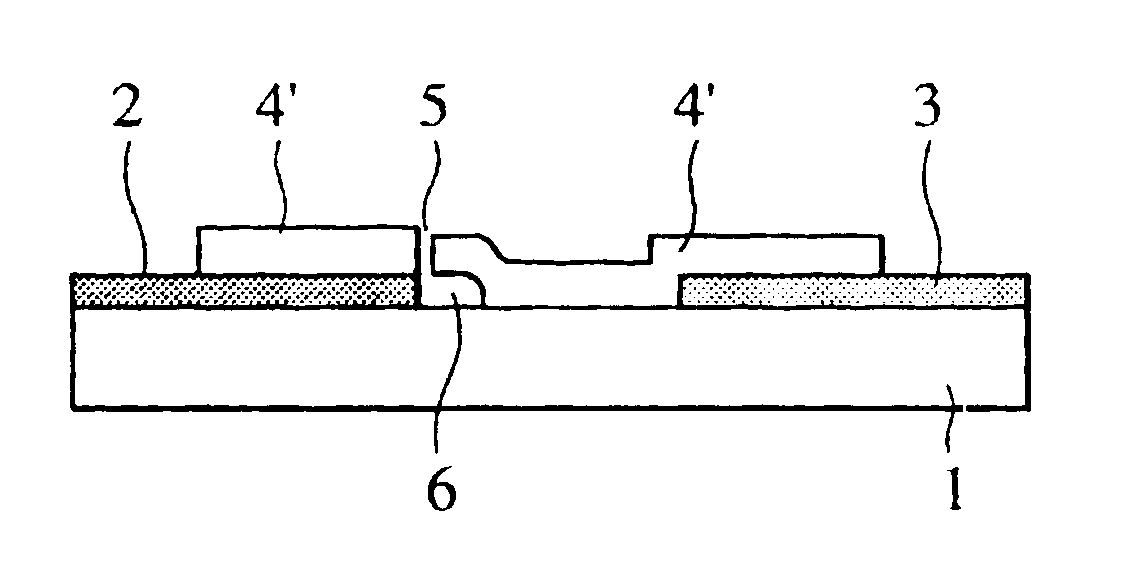
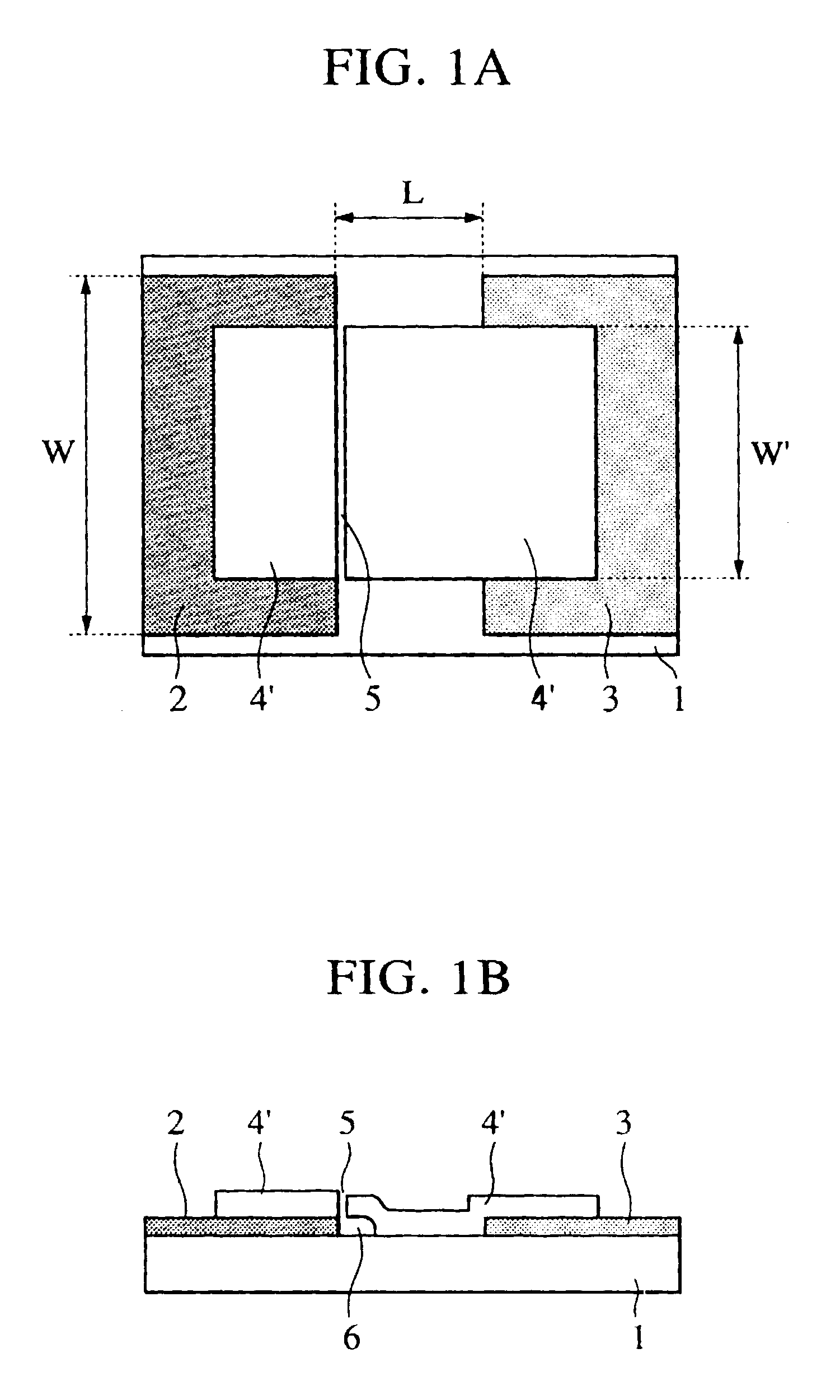
[0310]In this embodiment, an electron emitting device of the present invention shown in FIG. 1 is manufactured.

[0311]A glass substrate is used as the substrate 1 so that a laser beam can be transmitted through the substrate 1. Therefore, both the front and back of the glass substrate 1 can be irradiated with a laser beam. As the material for the opposing electrodes 2 and 3, platinum having a high heat resistance to laser irradiation, and particularly a high thermal conductivity is used. Aromatic polyimide is used for the polymer film 4.

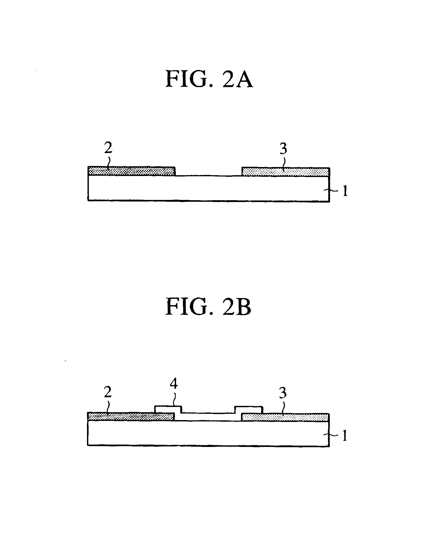
[0312]The method of manufacturing the electron emitting device of this embodiment is described with reference to FIGS. 1, 2 and 3.

[0313](Step 1)

[0314]A quartz glass substrate used as the substrate 1 is sufficiently cleaned with a detergent, pure water and an organic solvent, and a device electrode material is deposited on the substrate 1 by a vacuum deposition or sputtering method. Then, the electrodes 2 and 3 are formed by, for example, a photolithog...

second embodiment

[0329]In this embodiment, an electron emitting device is manufactured by basically the same steps as the first embodiment except that in this embodiment, the “resistance decreasing step” is performed by electron beam irradiation. Therefore, steps after step 2 of the first embodiment are described with reference to FIG. 8.

[0330](Step 3)

[0331]The substrate 1 on which the electrodes 2 and 3 and the polymer film 4 are formed is set in a vacuum container provided with an electron gun (not shown), and then the container is sufficiently evacuated. Then, the position of electron beam irradiation is set so that the center of the electron emitting device beam is applied to the electrode 3, and the electrode 3 is continuously irradiated with the electron beam (refer to FIGS. 8A and B). The conditions for electron beam irradiation include an acceleration voltage Vac of 10 kV. A spot diameter of the electron beam is set to 200 μm, and the center of the beam spot is set at a position 100 μm apart...


PUM


Abstract

The present invention provides an electron emitting device including electrodes disposed with a space therebetween on a surface of a substrate, a carbon film disposed between the electrodes and connected to one of the electrodes, and a gap disposed between the carbon film and the other electrode. In the gap, the distance between the edge of the carbon film connected to one of the electrode and the edge of the other electrode at an upper position apart from the surface of the substrate is smaller than that at the surface of the substrate. The present invention also provides an electron source and an image display device each including the electron emitting device.

Description

BACKGROUND OF THE INVENTION[0001]1. Field of the Invention[0002]The present invention relates to an electron emitting device, an electron source, an image display device, and methods of manufacturing these devices.[0003]2. Description of the Related Art[0004]Conventional electron emitting devices are roughly of two types, including thermionic-cathode electron-emitting devices, and cold-cathode electron-emitting devices. Example of cold-cathode electron-emitting devices include a field emission type (referred to as “FE type” hereinafter), a metal / insulator / metal type (referred to as “MIM type” hereinafter), a surface conduction type, and the like, types of electron-emitting devices.[0005]Known examples of FE type devices are disclosed in M. P. Dyke & W. W. Dolan, “Field Emission”, Advance in Electron Physics, 8, 89 (1956), C. A. Spindt, “Physical Properties of Thin-Film Field Emission Cathodes with Molybdenum Cones”, J. Appl. Phys., 47, 5248 (1976), and Japanese Patent Laid-Open No. ...

Claims


Application Information

Patent Timeline
IPC IPC(8): H01J9/02H01J1/02H01J1/316H01J29/04H01J31/12
CPCH01J9/027H01J1/316H01J1/30
Inventor KYOGAKU, MASAFUMIMIZUNO, HIRONOBUHAMAMOTO, YASUHIROMIYAZAKI, KAZUYA
Owner CANON KK
Why Eureka
Try Eureka