Silicon continuous casting method

a casting method and silicon technology, applied in the direction of silicon compounds, polycrystalline material growth, manufacturing tools, etc., can solve the problems high cost of high-quality silicon raw materials, and leakage of melt materials

Inactive Publication Date: 2006-02-07
SUMITOMO MITSUBISHI SILICON CORP
View PDF5 Cites 14 Cited by
  • Summary
  • Abstract
  • Description
  • Claims
  • Application Information

AI Technical Summary

Benefits of technology

[0042]As the heating source to form a silicon melt inside the bottomless crucible, it is desirable to use electromagnetic induction heating and plasma arc heating concurrently. During casting, the electromagnetic induction output is suppressed to prevent concave shaping of the solid-liquid interface, but reducing this to 0 will eliminate the repulsive force acting between the bottomless crucible and silicon melt and makes it more difficult to extract solidified ingots of silicon. That is, it is the most preferable mode to mainly use plasma arc heating during casting and reduce electromagnetic induction heating to a minimum necessary output to generate electromagnetic force to extract solidified ingots of silicon.

Problems solved by technology

However, high quality silicon raw materials are expensive, and therefore silicon raw materials of low quality with relatively high percentage of impurities are required from the standpoint of the manufacturing cost.
However, enhancing thermal insulation in such a way will increase the temperature of the surface of the ingot in the lower part of the bottomless crucible and when a certain temperature is exceeded, leakage of melt may occur due to breakage of the solidified shell.
In addition, when the concave shape of the solid-liquid interface grows noticeably, the solidified shell becomes thinner and it is more difficult to keep warm the side of the solidified ingot immediately after solidification and to increase the amount of heat radiation from the side, the length from the lower end of the induction coil to the lower end of the crucible which constitutes the cooling section of the bottomless crucible is increased.
As a result, heat loss of the ingot which faces the surface of the crucible over a wide range immediately after solidification is promoted, causing considerable deterioration of quality.
Thus, solubility of additional raw materials cannot be said to be sufficient.
In that case, it has been discovered that fixed heating of the central area of the silicon melt causes heat to be concentrated on the central area, making the concave shape of the solid-liquid interface grow noticeably and preventing sufficient improvement of the performance.
Furthermore, when continuous casting of silicon is performed by using transferred plasma heating concurrently with electromagnetic induction heating, it has also been discovered that the following problems occur in connection with the current-carrying path of the plasma current.
Attaching the plasma electrode on the ingot side to the extractor causes the solidified ingot of silicon to generate heat over the total length, but the total length of the ingot is not stable in case of continuous casting resulting in unstable heat generation.
This causes seriously adverse influences on the quality of the ingot.
This voltage increase deteriorates the thermal efficiency during casting and causes quite a big problem in manufacturing solidified ingots of silicon of high quality at low costs.
When power is supplied under the chamber, the solidified ingot of silicon is extracted from the chamber without decreasing its temperature and a drastic temperature variation may cause cracking on the surface.
To continue continuous casting, it is necessary to cut the solidified ingot of silicon under the chamber every time a certain length of ingot is cast, but since the temperature at the cut section increases, there is a danger that the cutting blade will not be able to withstand the heat, making the cutting difficult.

Method used


Image

  • Silicon continuous casting method
  • Silicon continuous casting method
  • Silicon continuous casting method

Examples


Embodiment Construction

[0058]With reference now to the attached drawings, embodiments of the present invention will be explained below.

[0059]A first silicon continuous casting method of the present invention will be explained with reference to FIG. 1 to FIG. 9.

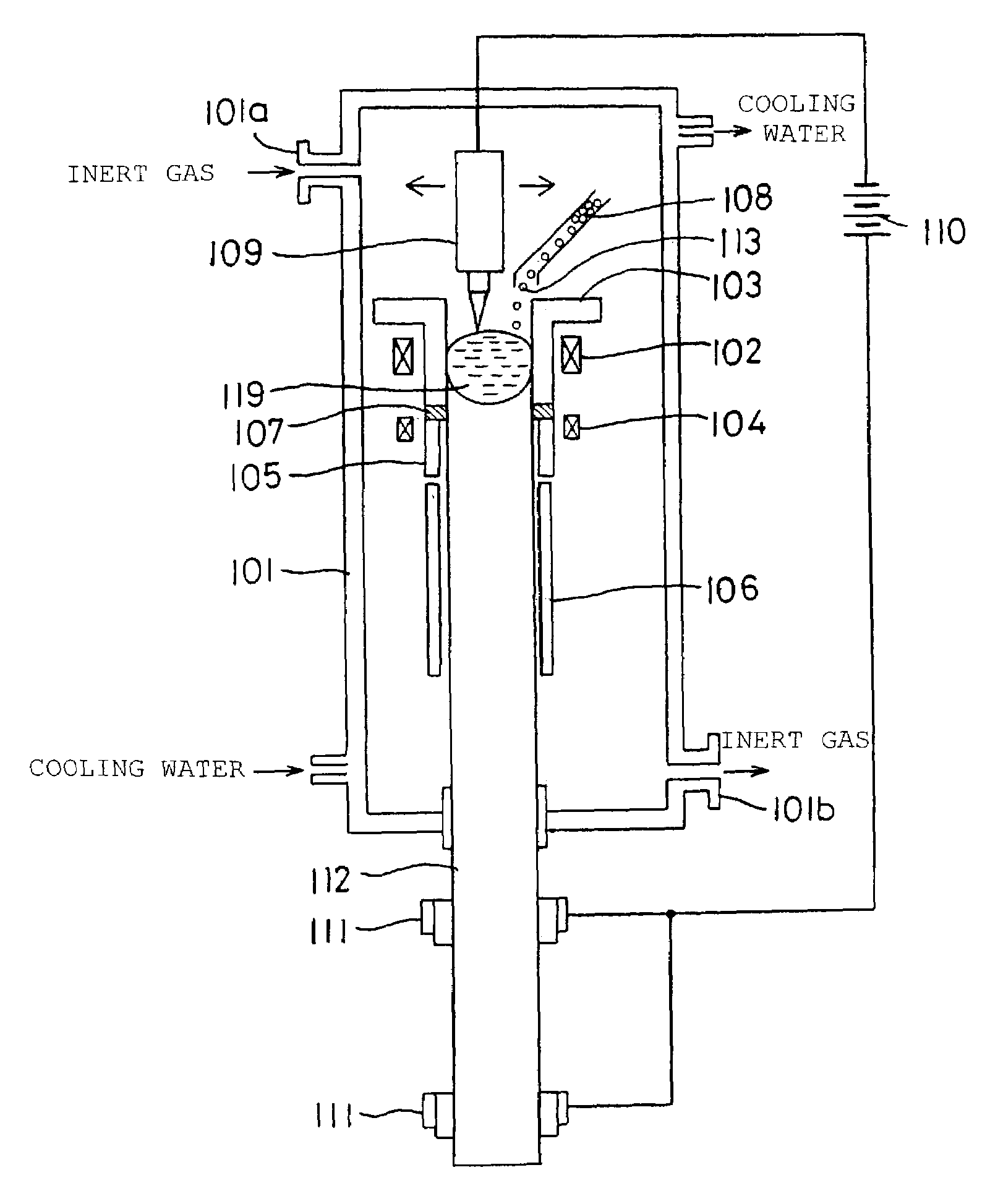
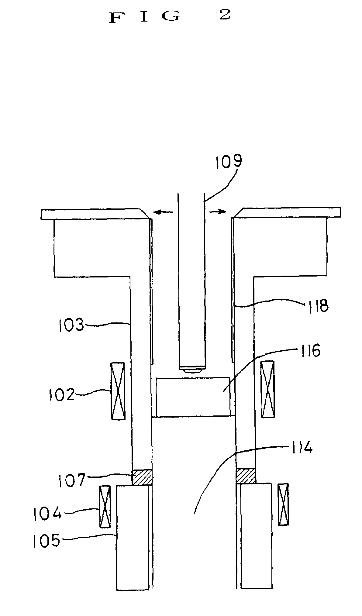
[0060]FIG. 1 is a block diagram of a continuous casting apparatus suitable for carrying out a first silicon continuous casting method of the present invention, FIG. 2 is a longitudinal cross-sectional view of the upper part of the apparatus showing an operation during initial melting, FIG. 3 is a longitudinal cross-sectional view of the upper part of the apparatus showing an operation during casting and FIG. 4 is an A—A line arrow view of FIG. 3.

[0061]As shown in FIG. 1, the continuous casting apparatus is provided with a chamber 101 to keep a casting atmosphere. To keep this casting atmosphere, an inert gas is circulated in the chamber 101 from a gas inlet 101a to a gas outlet 101b. Inside the chamber 101 is a square tubular bottomless crucible 103...


PUM

PropertyMeasurementUnit
temperatureaaaaaaaaaa
melting pointaaaaaaaaaa

Abstract

The present invention reduces temperature gradient in the direction of the radius of solidified ingots of silicon immediately after solidification, which has serious influences on the quality as a solar cell and improves the quality. Silicon raw materials are melted inside a bottomless crucible combined with an induction coil by electromagnetic induction heating. The silicon melt formed inside the bottomless crucible is allowed to descend and solidified ingots of silicon are manufactured continuously. Plasma heating by a transferred plasma arc torch is also used for melting the silicon raw materials. The plasma arc torch is moved for scanning along the inner surface of the bottomless crucible in the horizontal direction. A plasma electrode on the solidified ingot side to generate transferred plasma arc is allowed to contact the surface of the solidified ingot at positions where the temperature of the solidified ingot becomes 500 to 900° C.

Description

TECHNICAL FIELD[0001]The present invention relates to a silicon continuous casting method used for manufacturing ingots of silicon for a solar cell, etc.BACKGROUND ART[0002]A silicon wafer for a solar cell is conventionally manufactured by thinly slicing unidirectionally solidified ingots of silicon. The quality and cost of a silicon wafer are dependent on the quality and cost of solidified ingots of silicon. Thus, improving the quality of a silicon wafer and reducing the cost thereof will require that high quality unidirectionally solidified ingots of silicon should be manufactured at a low cost, and as this method, the applicant of the present invention has put a silicon continuous casting method using electromagnetic induction heating to practical use.[0003]The silicon continuous casting method using electromagnetic induction heating uses an electrically conductive bottomless crucible 3 which is placed inside an induction coil 2 and at least part in the axial direction of which i...

Claims


Application Information

Patent Timeline
Patent Type & Authority Patents(United States)
IPC IPC(8): C01B33/02C30B11/00
CPCC30B29/06C30B11/001
Inventor SASATANI, KENICHIKIMURA, NARITOSHIOHNISHI, MASAKAZU
Owner SUMITOMO MITSUBISHI SILICON CORP
Why Eureka
Try Eureka