Optical modulators

a technology of optical modulators and feedthrough portions, applied in non-linear optics, instruments, optics, etc., can solve the problems of low modulation efficiency, improve the microwave characteristic, increase the characteristic impedance of the feedthrough portion, and improve the microwave characteristic

Active Publication Date: 2006-02-21
NGK INSULATORS LTD
View PDF9 Cites 5 Cited by
  • Summary
  • Abstract
  • Description
  • Claims
  • Application Information

AI Technical Summary

Benefits of technology

[0041]The optical modulator of this embodiment relates to electrode configuration of so called asymmetric coplanar strip line type. The invention provides the advantageous effects described above. In the present aspect, the electrode configuration is of so called asymmetric coplanar strip line type, and the electrode gap in the modulating electrode is set at 19 μm or less (a half of 38 μm or less).
[0042]The width of a center electrode may be preferably larger for facilitating the electrical connection of the center electrode and a connector pin in a feedthrough portion. Moreover, a conductive layer may be provided on the surface of the supporting body to shield electromagnetic wave and to improve the microwave characteristic. In these cases, the characteristic impedance of the feedthrough portion of the optical modulator tends to be lowered, resulting in mismatching with the characteristic impedance Zi of the signal source. In the third and fourth aspects of the present invention, a low dielectric portion having a dielectric constant lower than that of the electrooptic material for the main body may be provided direct under the main body. It is thus possible to increase the characteristic impedance of the feedthrough portion of the optical modulator.
[0043]Further, when the first and / or second aspect of the present invention is applied in the third or fourth aspect of the present invention, the electrode gap may be further reduced (narrowed) to result in a lower driving voltage. This embodiment will be described below further in detail.
[0044]As the electrode gap is smaller, the characteristic impedance of microwave of the electrode is also lowered. In a prior optical modulator based on impedance matching at 50 Ω, the optical response of the modulator is considerably reduced in a low frequency band due to impedance mismatching. The modulation bandwidth is thus considerably narrowed.
[0045]It is possible to increase the characteristic impedance to a value near 50 Ω by reducing the thickness of the main body of the optical modulator as the electrode gap is reduced as described above. It is, however, difficult to reduce the thickness of the main body to a value of 3 μm or lower, because the mechanical strength of the main body is lowered and the mode size of the optical waveguide is reduced so that the connection loss with an optical fiber is increased. That is, a practical minimum value of the electrode gap is limited by a minimum value of the thickness of the main body which may be easily processed and utilized.
[0046]It is, however, possible to perform efficient modulation even in an optical modulator having a low characteristic impedance by optimizing the proportions of impedances according to the third and fourth aspects of the present invention. It is thus possible to further reduce the electrode gap beyond the limitation of minimum thickness of the main body. The driving voltage may be thus further reduced compared with the modulator applying only the first or second aspect of the present invention.

Problems solved by technology

However, in a high frequency band higher than 1 GHz, the modulation efficiency is generally low when the modulating electrode applies a modulating signal on light.

Method used


Image

  • Optical modulators
  • Optical modulators
  • Optical modulators

Examples


examples

[0080](Production)

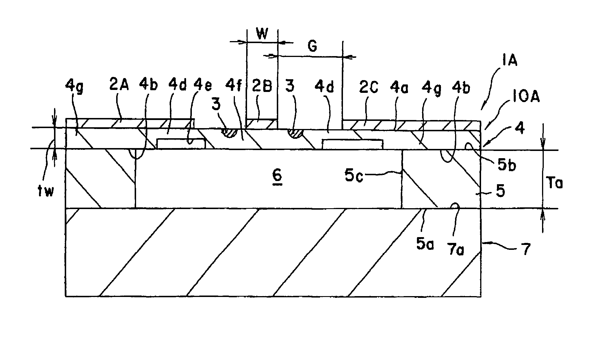
[0081]An optical modulator 1B shown in FIG. 6 was produced. An X-cut 3 inch wafer (made of LiNbO3 single crystal) was used as a substrate. An optical waveguide 3 of Mach-Zehnder type was formed in the surface area of the wafer by titanium diffusion and photolithography. The size of the optical waveguide 3 may be set at, for example, 10 μm at 1 / e2. The above described CPW electrode pattern was formed by electroplating.

[0082]A resist film was coated onto the one main face (surface) of the wafer-shaped bulk for the main body. The bulk was then adhered with a base substrate made of lithium niobate using a thermoplastic resin. The back face 4b of the main body was then subjected to horizontal polishing, high speed lapping and polishing (CMP). The thickness of the resulting main body was measured by means of a topographic measuring instrument, so that a desired thickness was obtained.

[0083]A sheet having a thickness of 50 μm and made of an epoxy thermosetting resin was s...


PUM

PropertyMeasurementUnit
thicknessaaaaaaaaaa
thicknessaaaaaaaaaa
thicknessaaaaaaaaaa

Abstract

An object of the present invention is to improve the modulation efficiency of an optical modulator in a high frequency band while satisfying the velocity matching condition. An optical modulator is provided having an optical waveguide for propagating light, an electrode for applying a voltage on the waveguide for modulating the light, a signal source electrically connected to the electrode and a terminating resistance electrically connected to the electrode. The signal source has a characteristic impedance Zi and the terminating resistance has an impedance Zl satisfying the formula (Zi<Zl). Alternatively, the signal source has a characteristic impedance Zi and the electrode has a characteristic impedance Zc satisfying the formula (Zi<Zc).

Description

CROSS-REFERENCE TO RELATED APPLICATIONS[0001]This application claims the benefits of Japanese Patent Application P2002-320930 filed on Nov. 5, 2002, and P2003-346736 filed on Oct. 6, 2003, the entireties of which are incorporated by reference.BACKGROUND OF THE INVENTION[0002]1. Field of the Invention[0003]The present invention relates to an optical modulator.[0004]2. Related Art Statement[0005]A traveling-wave optical modulator using lithium niobate (LiNbO3), lithium tantalate (LiTaO3) or gallium-arsenide (GaAs) for the optical waveguide has excellent properties and may realize a broadband modulation at a high efficiency. Lithium niobate and lithium tantalate are excellent ferroelectric materials having large electrooptic coefficients and can control light within a short optical path. Factors suppressing the modulation frequency of the traveling-wave optical modulator include velocity mismatch, dispersion, electrode conductor loss and dielectric loss.[0006]The assignee filed a Japan...

Claims


Application Information

Patent Timeline
Patent Type & Authority Patents(United States)
IPC IPC(8): G02F1/00G02F1/035G02F1/01
CPCG02F1/0356G02F1/0121
Inventor MITOMI, OSAMUAOKI, KENJIKONDO, JUNGOKONDO, ATSUO
Owner NGK INSULATORS LTD
Why Eureka
Try Eureka