Semiconductor device formed on (111) surface of a Si crystal and fabrication process thereof

a semiconductor device and surface technology, applied in semiconductor devices, digital storage, instruments, etc., can solve the problems of poor breakdown voltage characteristics or poor leakage current characteristics of the oxide film thus formed, deterioration of the device performance, and inability to form a mis transistor with a large driving power, etc., to achieve the effect of large driving power

Inactive Publication Date: 2006-03-14
OHMI TADAHIRO
View PDF18 Cites 46 Cited by
  • Summary
  • Abstract
  • Description
  • Claims
  • Application Information

AI Technical Summary

Benefits of technology

[0011]Accordingly, it is a general object of the present invention to provide a novel and useful semiconductor device and fabrication process thereof wherein the foregoing problems are eliminated.
[0012]Another object of the present invention is to provide an insulation film forming technology capable of forming a high-quality insulation film on a (111) surface of a Si crystal at a low temperature below about 550° C., a fabrication process of a semiconductor device on a (111) surface of a Si crystal by using such a insulation film forming technology, and a semiconductor device fabricated according to such a fabrication process.
[0017]According to the present invention, active atomic state oxygen O* are formed efficiently by activating O2 in Kr plasma excited by a microwave. By causing the atomic state oxygen O* to react, it becomes possible to form a Si oxide film having a quality superior to a silicon thermal oxide film formed at about 1000° C. on the (111) surface of a Si crystal. By using the Si oxide film thus formed as a gate insulation film, it becomes possible to form a high-performance semiconductor device or a semiconductor integrated circuit device on the (111) surface of the Si crystal. The (111) surface of the Si crystal may be the one defining the principal surface of the Si single crystal substrate or the one formed in a part thereof. Further, the (111) surface may be the one appearing at the surface of a polysilicon film.
[0018]According to the present invention, active hydrogen nitride radicals NH* are formed efficiently by activating NH3 or a mixed gas of N2 and H2 in microwave exited plasma of Ar or Kr. By causing the hydrogen nitride radicals NH3* to react, it becomes possible to form a silicon nitride film having a quality superior to a silicon thermal oxide film formed at about 1000° C. on the (111) surface of a Si crystal at a low temperature of 550° or less. The silicon nitride film thus formed can be used as a high-dielectric gate insulation film and it becomes possible to form a high-performance semiconductor device or a high-performance semiconductor integrated circuit device on the (111) surface of the Si crystal. It should be noted that the (111) surface of the Si crystal may be the one defining the principal surface of a Si single crystal substrate or the one formed in a part thereof. Further, the (111) surface may be the one appearing at the surface of a polysilicon film.
[0019]According to the present invention, it becomes possible to form a high-quality Si oxide film or a silicon nitride film on the (111) surface formed at the corner part of the device isolation groove of an STI structure. As a result, it becomes possible to reduce the leakage current of the STI structure and the breakdown characteristic thereof without increasing the width of the device isolation groove. As a result, it becomes possible to improve the electric property and the reliability in the semiconductor device that has such an STI structure.
[0021]Further, the present invention enables formation of high-quality gate oxide film or gate nitride film on a Si film formed of Si crystals preferentially oriented in the <111> direction. Thus, it becomes possible to realize a polysilicon transistor or a thin film transistor having a large driving power. Further, it becomes possible to realize a three-dimensional integrated circuit device in which functional devices are stacked in plural layers.

Problems solved by technology

When a thermal oxidation process is applied to a Si substrate having a surface orientation other than the (100) surface for forming a gate oxide film, there arises various problems in the gate oxide film such as increased surface state density at the oxide / Si substrate interface as compared with case of forming the Si oxide film on the (100)-oriented Si substrate.
Further, the oxide film thus formed suffers from the problem of poor breakdown voltage characteristics or poor leakage current characteristics.
On the other hand, it is not possible to form a MIS transistor having a large driving power on a Si substrate having a different surface orientation.
However, the use of high temperature process that requires a temperature of 550° C. or more in the device fabrication process raises the problem of deterioration of device performance caused by reaction between the metal layer and the semiconductor layer.
Further, the use of high-temperature annealing process tends to facilitate diffusion of impurity elements introduced into the active region of the semiconductor layer, and there arises a difficulty in controlling the impurity distribution profile accurately.
However, there has been no known process that enables formation of a high-quality high-dielectric film having a small surface state density and excellent electric property on a (111) surface of a Si crystal at low temperature.
In a semiconductor integrated circuit having such an STI structure, there arises a problem in that the thickness of an Si oxide film formed by a thermal oxidation process is tend to be reduced at the corner part of the device isolation groove as compared with the flat surface of the Si substrate.
Associated therewith, the quality of the Si oxide film is deteriorated in such a corner part.
Thus, there has been a reliability problem in the conventional semiconductor integrated circuit devices that uses an STI structure, such as degradation of leakage current characteristic or degradation of breakdown characteristic, particularly at the corner part of the STI structure.
In spite of such a measure, however, it has not been successful to suppress the degree of decrease of the film thickness below about 30%, and thus, the problem of increased leakage current or degradation of breakdown characteristic of the oxide film in the thinned part thereof has not been overcome.
Further, the device having such a tapered device isolation groove has a drawback of increased width of the device isolation groove, and associated problem of reduced effective area on which semiconductor devices such as a transistor are formed.
Thereby, increase of integration density of the semiconductor integrated circuit device has been impeded.
As long as conventional thermal oxidation process is used, it has been difficult to form a high-quality silicon gate oxide film on such a polysilicon film having the preferred orientation in the direction.
Thus, it has been difficult to form a high-speed semiconductor device of short gate length on a Si substrate formed on an insulation film such as a polysilicon film, and thus, it has been difficult to realize a three-dimensional integrated circuit by stacking a number of insulation films each carrying a semiconductor device.

Method used


Image

  • Semiconductor device formed on (111) surface of a Si crystal and fabrication process thereof
  • Semiconductor device formed on (111) surface of a Si crystal and fabrication process thereof
  • Semiconductor device formed on (111) surface of a Si crystal and fabrication process thereof

Examples


first embodiment

[First Embodiment]

[0087]Next, a description will be made on a semiconductor device according to a first embodiment of the present invention that uses a two-layer structure of low-temperature oxide film and nitride film formed in a plasma for the gate insulation film.

[0088]In the present embodiment, the substrate processing apparatus of FIG. 1 is used for the formation of the oxide film and nitride film. Thereby, Kr is used for the plasma gas.

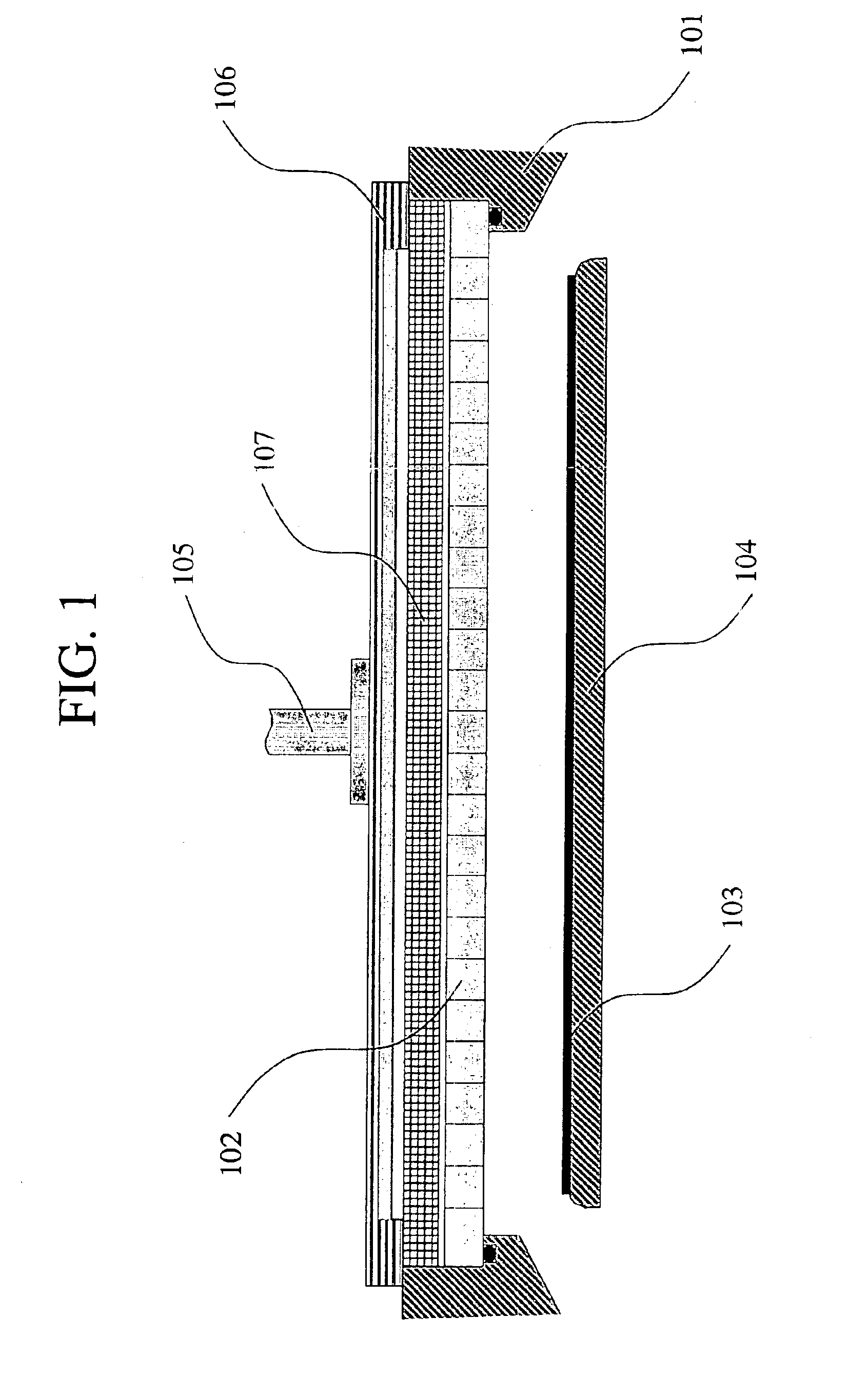
[0089]Referring to FIG. 1, the vacuum vessel (processing chamber) 101 is evacuated to a vacuum state and a Kr gas and an O2 gas are introduced into the processing chamber 102 from the shower plate 102 such that the pressure inside the processing chamber 101 is set to about 1 Torr. Further, the temperature of the silicon wafer is set to about 450° C.

[0090]Next, a microwave having the frequency of 2.45 GHz is introduced into the processing chamber from the coaxial waveguide 105 through the radial line slot antenna 106 and the dielectric plate 107,...

second embodiment

[Second Embodiment]

[0100]FIG. 11A shows a typical conventional STI structure.

[0101]Referring to FIG. 11A, the STI structure is formed by the steps of forming a device isolation groove by applying a plasma etching process to the surface of a Si substrate 1003, depositing a Si oxide film 1002 on the surface of the Si substrate 1003 thus formed with the device isolation groove by a CVD process, and planarizing the Si oxide film 1002 thus deposited by a CMP process, and the like, to remove the Si oxide film from the surface of the Si substrate 1003.

[0102]After the foregoing polishing step by the CMP process, the exposed Si substrate surface is subjected to a sacrificing oxidation process at 800-900° C., and the Si oxide film formed as a result of the sacrificing oxidation process is etched by an agent containing HF. Thereby, a highly clean Si substrate is obtained.

[0103]The clean substrate surface thus obtained is further cleaned by using an RCA cleaning process, and the like, and a gat...

third embodiment

[Third Embodiment]

[0110]FIG. 12 is a cross-sectional diagram showing the schematic construction of a ferroelectric memory device according to a third embodiment of the present invention.

[0111]Referring to FIG. 12, the ferroelectric memory device is constructed on a Si substrate in which a p-type well 1101 is formed, wherein the p-type well 1101 is formed with a source region 1102 and a drain region 1102′ of n-type. Further, a Si nitride film 1103 is formed on the Si substrate with a thickness of 5 nm as the gate insulation film, wherein the nitride film 1103 is formed by the foregoing Ar / NH3 plasma processing conducted at the temperature of 400° C. Further, a polysilicon gate electrode 1104 of n-type is formed on the gate insulation film 1103.

[0112]Further, a Si nitride film 1105 is formed on the polysilicon gate electrode 1104 with a thickness of 5 nm by conducting the foregoing Ar / NH3 plasma nitriding processing at the temperature of 400° C., and a ferroelectric film 1106 of SrTaN...


PUM

PropertyMeasurementUnit
temperatureaaaaaaaaaa
angleaaaaaaaaaa

Abstract

A semiconductor device includes a Si crystal having a crystal surface in the vicinity of a (111) surface, and an insulation film formed on said crystal surface, at least a part of said insulation film comprising a Si oxide film containing Kr or a Si nitride film containing Ar or Kr.

Description

CROSS REFERENCE TO RELATED APPLICATIONS[0001]The present invention is based on Japanese patent application 11-376170 filed on Nov. 30, 1999, the entire contents thereof being incorporated herein by reference.BACKGROUND OF THE INVENTION[0002]The present invention generally relates to semiconductor devices and more particularly to a semiconductor device formed on a (111) surface of a Si crystal and fabrication process thereof.[0003]A gate insulation film of a MIS (metal / semiconductor / Si) transistor is subjected to various stringent requirements with regard to electric properties, including low leakage current, small surface state density, large hotcarrier resistance, and the like. Further, such a gate insulation film is required to provide high reliability. In order to meet for these stringent demands, it has been practiced conventionally to form the gate insulation film by a thermal oxidation of a Si substrate surface at a temperature of 800° C. or more.[0004]However, a satisfactory ...

Claims


Application Information

Patent Timeline
Patent Type & Authority Patents(United States)
IPC IPC(8): H01L29/94H01L21/316G11C11/16H01L21/28H01L21/318H01L21/336H01L21/8246H01L21/8247H01L27/12H01L29/04H01L29/49H01L29/51H01L29/786H01L29/788
CPCH01L29/7883H01L21/28194H01L21/28202H01L21/28211H01L21/28291H01L27/11521H01L27/11585H01L27/1159H01L27/1203H01L29/045H01L29/4908H01L29/513H01L29/518H01L29/66825H01L29/78603H01L29/78612H01L21/28185G11C11/16H01L21/28238H01L29/7833H01L29/40111H10B51/00H10B51/30H10B41/30
Inventor OHMISUGAWA, SHIGETOSHISEKINE, KATSUYUKISAITO, YUJI
Owner OHMI TADAHIRO
Why Eureka
Try Eureka