Methods of processing of gallium nitride

a gallium nitride and processing method technology, applied in the direction of polycrystalline material growth, crystal growth process, manufacturing tools, etc., can solve the problems of difficult to obtain high-quality gan film on sic, poor thermal conductivity of sapphire, and high cost of si

Inactive Publication Date: 2006-03-21
ALLEGIS TECH
View PDF14 Cites 63 Cited by
  • Summary
  • Abstract
  • Description
  • Claims
  • Application Information

AI Technical Summary

Problems solved by technology

Unlike other LED material systems (e.g., indium phosphide, gallium arsenide), GaN is generally grown on high quality sapphire (Al2O3) or silicon carbide (SiC) substrates, since high quality GaN wafers are not commercially available.
SiC is much more expensive than sapphire, and it is difficult to obtain high quality GaN films on SiC due to lower SiC quality as compared to sapphire.
Unfortunately, sapphire is a poor thermal conductor.
This presents difficulties in removing heat from the LED chip while it is in an operating state.
The higher the electrical input current, the more heat is generated in the chip, and the hotter the chip becomes, due to the limited thermal conductance of the sapphire substrate.
This problem is greatly exacerbated with increasing LED chip size, since these larger chips required much higher input currents to operate.
In fact, inefficient heat sinking ability is one of the limiting factors in large area LED brightness.
Chip temperature significantly affects the device lifetime and stability.
These packaging methods both increase costs and potentially reduce yields.
Furthermore, with ever increasing chip size and input power, these techniques may not be sufficient in removing enough thermal energy from the LED chip to keep operating temperatures stable and low.
GaN is both thermally and electrically insulating, a non-desirable trait.
At such energy densities, the beam size is limited to approximately 2 cm2 due to power limitations on commercially available lasers.
Generally, the first delamination produces high quality films, but high stresses build up at the interface between delaminated and non-delaminated areas.
These stresses can produce significant numbers of cracks in the GaN film during subsequent delamination cycles.
Such cracks significantly decrease yields in subsequent processing of the GaN film.
If these trenches are not etched completely through the GaN, then the chip-to-chip isolation is not very effective, and cracks still propagate from chip to chip.
If the trenches are etched completely through the GaN layer, then isolation is effective, but the support wafer bonding layer is exposed to the laser, thereby becoming weakened, leading to potential delamination of the support wafer prior to complete laser processing.
This conventional approach of applying the phosphor during packaging significantly complicates the packaging process, and limits the use of solid state white light sources.
Furthermore, over time the phosphor layer often interacts with the GaN chip, the wire bonds, or the epoxy used to encapsulate the LED package, resulting in degradation over time and reduced lifetimes.
GaN is generally grown on a very high quality sapphire (Al2O3) substrate, which is both thermally and electrically insulating, a non-desirable trait.
Generally, it is difficult to make good ohmic contact to the p-doped GaN layer, and the metallurgy available for such a contact is limited.

Method used


Image

  • Methods of processing of gallium nitride
  • Methods of processing of gallium nitride
  • Methods of processing of gallium nitride

Examples


Embodiment Construction

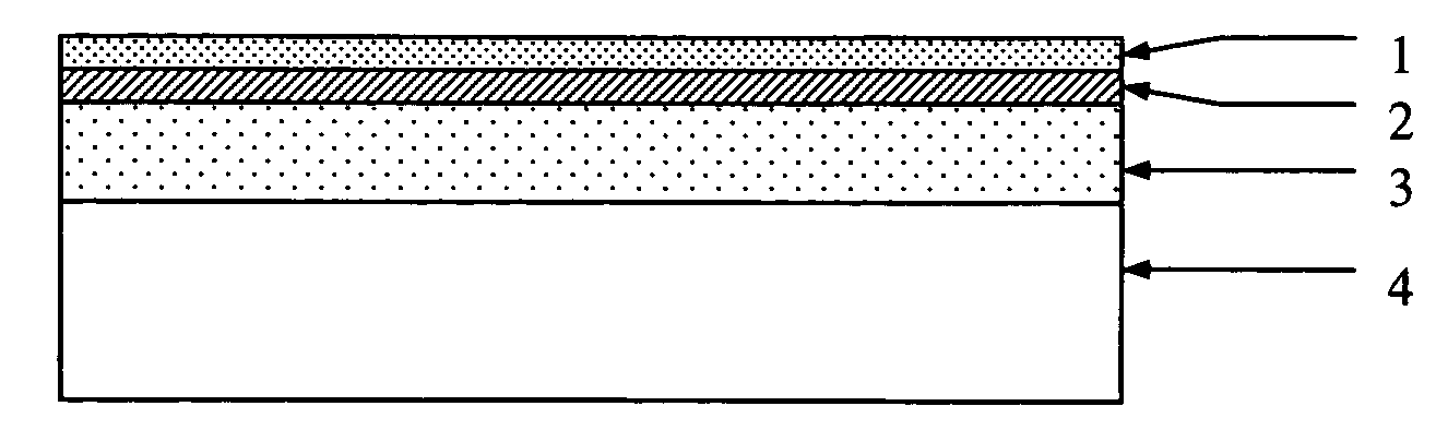
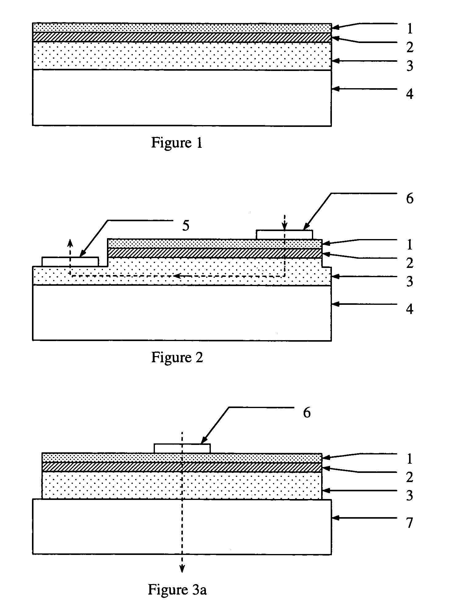
[0041]In one embodiment, GaN epitaxial films grown for LED applications consist of three main, sequentially grown layers (FIG. 1), each of which can be further subdivide into numerous additional layers. The main layers consist of a moderately conductive p-doped GaN layer (1), a light emitting InGaN quantum well (either single or multiple) layer (2), and a conductive n-doped GaN layer (3). Due to the rectifying nature of the GaN p-n junction, such a GaN film can only conduct electrical current from the p-layer (1), through the quantum well (QW) layer (2), into the n-layer (3), not in the other direction. Light will emit from the QW layer only if sufficient current is passed through it, as described above. Consequently, a GaN LED device requires a contact pad to both the n- and p-layers (1,3) through which to deliver this activating current.

[0042]In the conventional GaN on sapphire LED (FIG. 2), some of the GaN must be removed to make contact to the n-layer (3) via the n-pad (5). This...


PUM

PropertyMeasurementUnit
melting pointaaaaaaaaaa
sizeaaaaaaaaaa
wavelengthsaaaaaaaaaa

Abstract

A method for improving thermal dissipation in large gallium nitride light emitting diodes includes replacing sapphire with a better thermal conductor resulting in more efficient removal of thermal energy. A method for achieving a reliable and strong temporary bond between a GaN epitaxial layer and a support wafer. A method for transferring an epitaxial film from a growth substrate to a secondary substrate. An excimer laser initiates film delamination from the growth substrate. The laser beam is shaped by a shadow mask and aligned to an existing pattern in the growth substrate. A method for fabricating a LED that radiates white spectrum light. A phosphor that radiates a white spectrum after excitation in the blue or UV spectrum onto the GaN epitaxial wafer prior to die separation and packaging. A method for depositing a metal substrate onto a GaN epitaxy layer.

Description

[0001]The present application claims priority from U.S. Provisional Patent Applications including the following Ser. Nos.: Ser. No. 60 / 492,720 filed Aug. 4, 2003; Ser. No. 60 / 489,350 filed Jul. 22, 2003; Ser. No. 60 / 487,896 filed Jul. 14, 2003; Ser. No. 60 / 492,713 filed Aug. 4, 2003; and Ser. No. 60 / 487,417 filed Jul. 14, 2003. The disclosure of these provisional applications is incorporated herein by reference.BACKGROUND OF THE INVENTION[0002]1. Field of the Invention[0003]The present invention relates generally to the field of high power light emitting diodes, and epitaxial films, and more particularly to high power gallium nitride on sapphire light emitting diodes, and to the transfer of GaN films from a growth substrate to a secondary substrate, and to vertical gallium nitride and while gallium nitride diodes.[0004]2. Description of the Prior Art[0005]Gallium nitride (GaN) based light emitting diodes (LEDs) are an important source of solid state lighting in the UV through Green ...

Claims


Application Information

Patent Timeline
Patent Type & Authority Patents(United States)
IPC IPC(8): H01L21/00C30B1/00H01LH01L21/20H01L21/36H01L33/00H01L33/64
CPCB23K26/409C30B25/02C30B29/406H01L33/0079H01L33/641H01L2224/48091H01L2224/48247H01L2924/10253H01L2924/12041H01L2224/48257H01L2924/00014H01L2924/00B23K26/40B23K2103/172H01L33/0093
Inventor URBANEK, WOLFRAM
Owner ALLEGIS TECH
Why Eureka
Try Eureka