Method for making thin-film semiconductors based on I-III-VI2 compounds, for photovoltaic applications

a technology of i-iii-vi2 and compound, applied in the field of semiconductor thin film deposition, can solve the problems of difficult crystallization of cigs, low use efficiency, and high cost of evaporation, and achieve satisfactory crystallization of the layer, and limit the exodiffusion of vi elements.

Inactive Publication Date: 2006-04-11
ELECTRICITE DE FRANCE +1
View PDF3 Cites 106 Cited by
  • Summary
  • Abstract
  • Description
  • Claims
  • Application Information

AI Technical Summary

Benefits of technology

[0036]rapidly annealing this precursor, so that the kinetics of the processing are fast enough to limit exodiffusion of the VI element (owing to its volatility) during the annealing, while allowing satisfactory crystallization of the layer.

Problems solved by technology

It is therefore difficult to obtain crystallized CIGS with the intended composition (close to the I-III-VI2 stoichiometry) without adding selenium for the annealing of the precursor layer.
Evaporation is an expensive technique which is difficult to use on the industrial scale, however, particularly because of nonuniformity problems with the thin-film deposits over large surface areas and a low efficiency of using the primary materials.
Cathodic sputtering is more suitable for large surface areas, but it requires very expensive vacuum equipment and precursor targets.
The difficulties which are encountered, however, relate to controlling the quality of the electrodeposited precursors (composition, morphology) and processing them with a view to providing adequate electronic properties for the photovoltaic conversion.
Such annealing, however, is relatively time-consuming (of the order of one to a few hours).
When it is deposited by sputtering and has a heterogeneous structure in sheets, however, the thin film is not good at withstanding abrupt rises in temperature, especially in mechanical terms.
Since the thermal expansion coefficient of the layer is spatially inhomogeneous, delamination problems occur with this layer during the annealing step.
Although advantageous, such a procedure is therefore not yet completely satisfactory.
A difficulty arises when carrying out such methods.
This effect is commensurately more problematic when there are a large number of elements in the alloy to be obtained (ternary CIS, quaternary CIGS, etc.).

Method used


Image

  • Method for making thin-film semiconductors based on I-III-VI2 compounds, for photovoltaic applications
  • Method for making thin-film semiconductors based on I-III-VI2 compounds, for photovoltaic applications
  • Method for making thin-film semiconductors based on I-III-VI2 compounds, for photovoltaic applications

Examples


Embodiment Construction

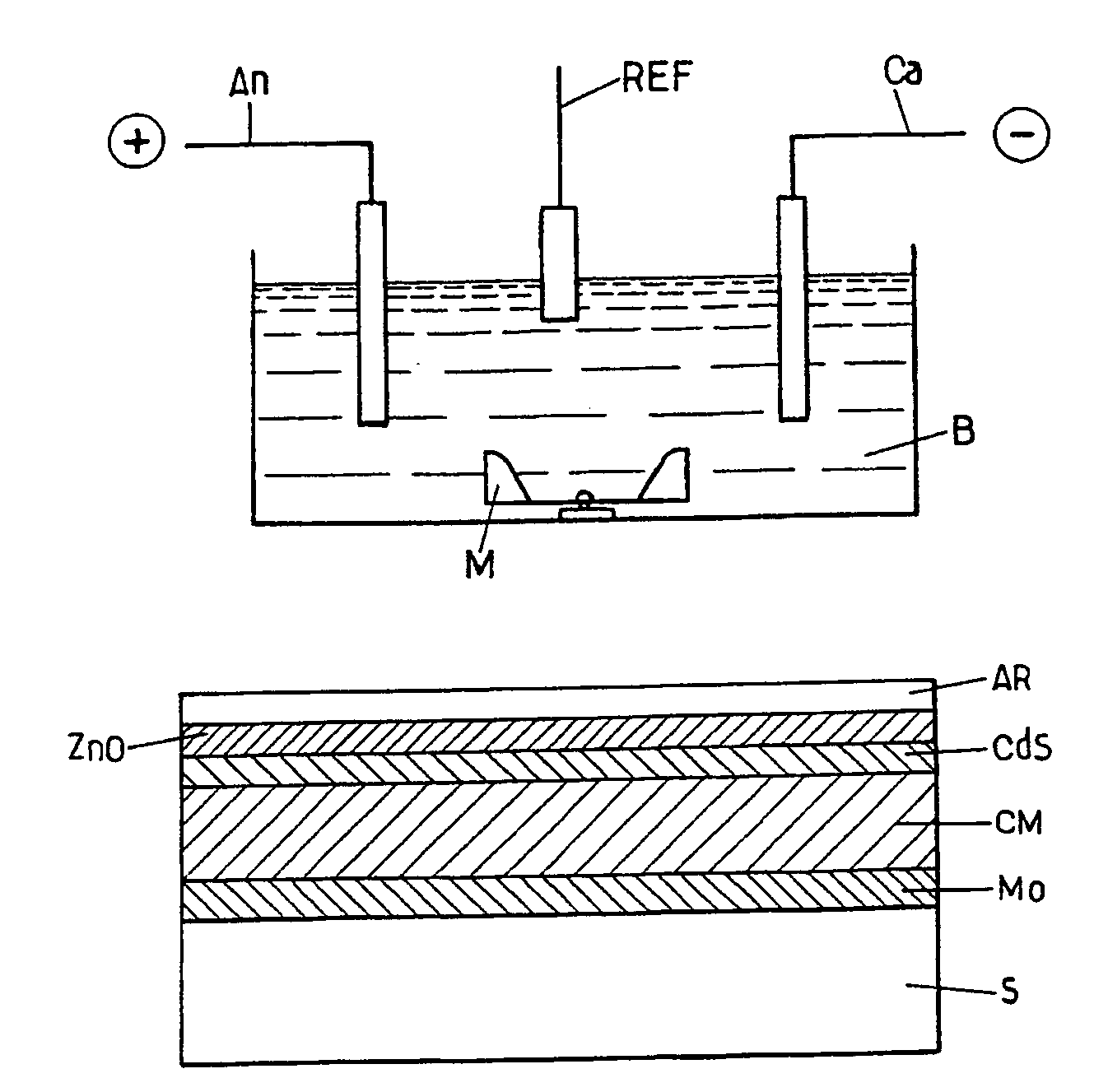
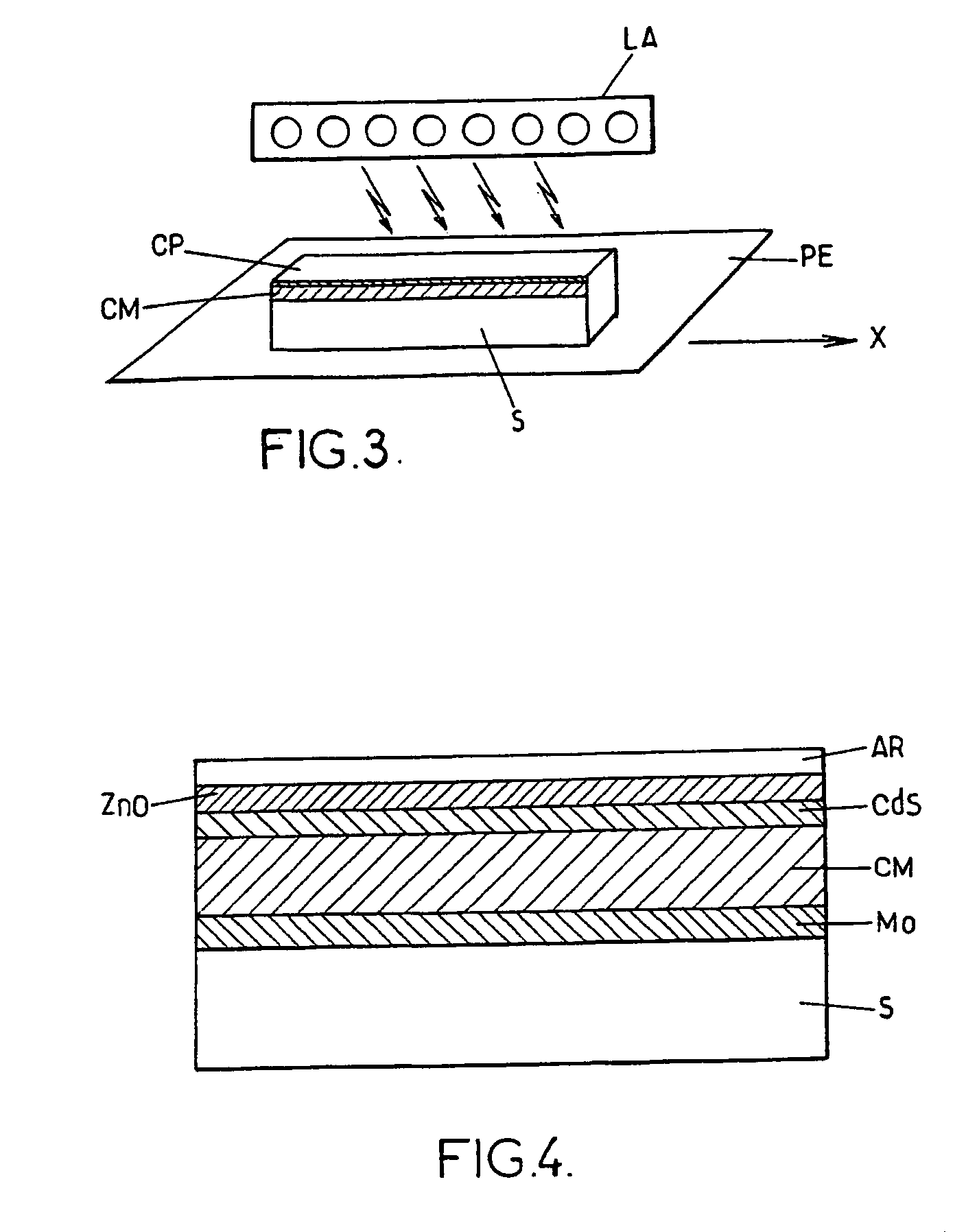
[0052]Referring to FIG. 1, thin films of copper and indium diselenide are obtained at room pressure and temperature by electrodeposition of a precursor film CM on a glass substrate S previously covered with molybdenum Mo (FIG. 4). Advantageously, the substrate S is initially covered with an additional electronic conductive layer, for example metallic or in an oxide form (not shown). This conductive layer may furthermore rest on one or more sublayers used for a specific application (diffusion barrier, mirror or the like) in the fabrication of photovoltaic cells.

[0053]Referring to FIG. 1, the electrodeposition is carried out in a bath B containing an indium salt, a copper salt and dissolved selenium oxide. In order to obtain a CIGS thin film whose general composition corresponds substantially to CuGaxIn1−xSe2 (with x between 0 and 1), it will be understood that the bath may furthermore contain a gallium salt. In an even more sophisticated variant, sulfur salts (for example sulfite or ...


PUM

PropertyMeasurementUnit
temperatureaaaaaaaaaa
band gapaaaaaaaaaa
band gapaaaaaaaaaa

Abstract

The invention concerns a method for making thin-film CIGS which consists in: electrochemically depositing on a substrate a layer of stoichiometry close to CuInSe2; then rapidly annealing said layer from a light source with pulses of sufficient power to recrystallize CIS. Advantageously, the electrodeposited elements are premixed. Thus, after the deposition step, a homogeneous matrix is obtained which can support sudden temperature increases during the rapid annealing.

Description

CROSS REFERENCE TO RELATED APPLICATIONS[0001]This application is a national phase of PCT / FR03 / 01282 filed Apr. 23, 2003 which claims priority to French Patent Application No. :02 05362 filed Apr. 29, 2002BACKGROUND OF THE INVENTION[0002]The invention concerns the field of semiconductor thin film deposition for photovoltaic applications.[0003]Thin films of copper and indium and / or gallium diselenide and / or disulfide (CIGS) are deposited on a substrate in order to fabricate photovoltaic cells. Such compounds of general formula CuGaxIn1−xSe2−ySy (with x between 0 and 1 and y between 0 and 2) are regarded as highly promising and could constitute the next generation of thin-film solar cells. CIGS semiconductor materials have a direct band gap of between 1.0 and 1.6 eV, which permits strong absorption of solar radiation in the visible range. Record conversion efficiencies of more than 18% have recently been obtained with cells of small surface areas.[0004]CIGS are also referred to as I-II...

Claims


Application Information

Patent Timeline
Patent Type & Authority Patents(United States)
IPC IPC(8): H01L21/477C25D5/50C25D7/00H01L31/032H01L31/04H01L31/18
CPCH01L31/0322H01L31/1872H01L31/1864Y02E10/541Y02P70/50
Inventor TAUNIER, STEPHANEKERREC, OLIVIERMAHE, MICHELGUIMARD, DENISBEN-FARAH, MOEZLINCOT, DANIELGUILLEMOLES, JEAN-FRANCOISGRAND, PIERRE-PHILIPPECOWACHE, PIERREVEDEL, JACQUES
Owner ELECTRICITE DE FRANCE
Why Eureka
Try Eureka