Methods for making a dielectric stack in an integrated circuit

a technology of integrated circuits and dielectric stacks, which is applied in the direction of coatings, transistors, chemical vapor deposition coatings, etc., can solve the problems that dielectric stacks have been of little practical benefit for current commercial process flows, and achieve excellent interfacial properties, facilitate advanced materials, and speed up overall deposition rates

Inactive Publication Date: 2006-05-02
ASM INTERNATIONAL
View PDF19 Cites 57 Cited by
  • Summary
  • Abstract
  • Description
  • Claims
  • Application Information

AI Technical Summary

Benefits of technology

[0008]The dielectric structure is positioned between a first conductor and a second conductor. Aluminum oxide and lanthanide oxides have been found particularly beneficial as interface layers between doped semiconductor structures, such as a doped silicon substrate in a transistor structure, and other dielectric materials. Furthermore, their excellent interfacial properties facilitate advanced materials. For example, aluminum oxide has been found particularly advantageous between high-k materials and poly-SiGe gate electrodes. During CVD of SiGe, nucleation over ALD Al2O3 during initial phases of deposition was found superior to that over SiO2, thus speeding overall deposition rates. Other gate electrode materials may also be made possible due to superior nucleation of depositions thereover and protection against corrosion and impurit

Problems solved by technology

However, due to the slowness of the process (depositing one atomic layer of material per cycle), ALD has been of little practical benefit for current commercial process flows.

Method used


Image

  • Methods for making a dielectric stack in an integrated circuit
  • Methods for making a dielectric stack in an integrated circuit
  • Methods for making a dielectric stack in an integrated circuit

Examples


example 1

ALD of Aluminum Oxide from (CH3)3Al and Water

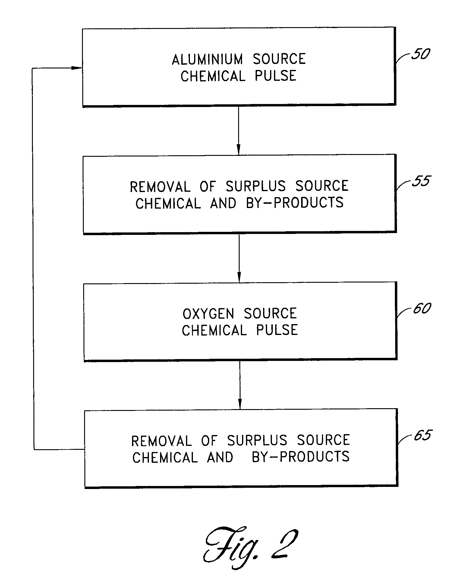
[0066]With reference again to FIG. 2, in a preferred embodiment, the aluminum source pulse 50 comprises trimethyl aluminum or TMA) ((CH3)3Al) fed into the reaction space. TMA chemisorbs on hydroxyl (—OH) groups on the substrate surface. Methane is released as a byproduct. The self-saturating surface reaction leaves a methyl-terminated aluminum oxide layer on the surface. The removal 55 comprises flowing inert gas flow to purge residual TMA and methane from the reaction space. The oxygen source pulse 60 comprises a water pulse that reacts with the methyl groups on aluminum oxide. The self-saturating surface reaction leaves a hydroxyl-terminated aluminum oxide layer on the substrate surface and methane gas is released as a byproduct. The second removal 65 also comprises flowing inert gas to purge residual water and methane from the reaction space. The substrate surface is now ready to receive the next TMA pulse. Alternating TMA and H2O reac...

example 2

ALD Processes Using Aluminum Beta-Diketonates

[0076]Aluminum acetylacetonate, i.e. Al(acac)3, and tris-(2,2,6,6-tetramethyl-3,5-heptanedionato)aluminum, i.e. Al(thd)3, react slowly with water. In the process aluminum oxide is formed and Hacac or Hthd vapor is released. Faster surface reactions are possible when using ozone as an oxygen source. However, ozone is preferably used only for the growth of the top interfacial aluminum oxide layer, as noted above in the discussion of preferred oxygen source materials, to avoid oxidation of the underlying substrate.

example 3

Replacing a SiO2 Interface Layer with Al2O3 by an Exchange Reaction

[0077]An ALD reactor or a CVD reactor is used for the process. A substrate with a silicon dioxide surface is placed into the reaction space. The pressure can be atmospheric, but preferably the pressure of the reaction space is adjusted to about 1–10 mbar. The substrate temperature is adjusted to between about 300° C. and 400° C. Vaporized aluminum compound, preferably aluminum halide and more preferably aluminum chloride, is contacted with the substrate surface for about two minutes.

[0078]When AlCl3 vapor is contacted with a SiO2 surface, solid Al2O3 is formed on the surface and SiCl4 vapor is formed. The Gibb's free energy of this reaction is favorable for the formation of aluminum oxide.

1.5SiO2(s)+2AlCl3(g)→Al2O3(s)+1.5SiCl4(g) ΔGf(300° C.)=−52 kJ [  2]

[0079]The completion of the exchange reaction can be monitored, e.g. with a quadrupole mass spectrometer located at the exhaust side of the reaction space. The react...


PUM

PropertyMeasurementUnit
Temperatureaaaaaaaaaa
Timeaaaaaaaaaa
Timeaaaaaaaaaa

Abstract

An ultrathin aluminum oxide and lanthanide layers, particularly formed by an atomic layer deposition (ALD) type process, serve as interface layers between two or more materials. The interface layers can prevent oxidation of a substrate and can prevent diffusion of molecules between the materials. In the illustrated embodiments, a high-k dielectric material is sandwiched between two layers of aluminum oxide or lanthanide oxide in the formation of a transistor gate dielectric or a memory cell dielectric. Aluminum oxides can serve as a nucleation layer with less than a full monolayer of aluminum oxide. One monolayer or greater can also serve as a diffusion barrier, protecting the substrate from oxidation and the high-k dielectric from impurity diffusion. Nanolaminates can be formed with multiple alternating interface layers and high-k layers, where intermediate interface layers can break up the crystal structure of the high-k materials and lower leakage levels.

Description

REFERENCE TO RELATED APPLICATIONS[0001]The present application is a divisional of non-provisional application Ser. No. 09 / 945,463, filed Aug. 31, 2001, entitled METHODS FOR MAKING A DIELECTRIC STACK IN AN INTEGRATED CIRCUIT, now U.S. Pat. No. 6,660,660. and claims the priority benefit under 35 U.S.C. § 119(e) to prior provisional application No. 60 / 239,040, filed Oct. 10, 2000, entitled METHOD OF DEPOSITING OXIDE THIN FILMS, provisional application No. 60,244,789, filed Oct. 31, 2000 entitled ALUMINUM OXIDE INTERFACE FILMS AND METHODS THEREFOR, and provisional application No. 60 / 247,115, filed Nov. 10, 2000, entitled DIELECTRIC INTERFACE FILMS AND METHODS THEREFOR.FIELD OF THE INVENTION[0002]The present invention relates generally to thin dielectric films in integrated circuits, and more particularly to interface layers for dielectric thin films.BACKGROUND AND SUMMARY OF THE INVENTION[0003]Atomic Layer Deposition (ALD) is a self-limiting process, whereby alternated pulses of reactio...

Claims


Application Information

Patent Timeline
IPC IPC(8): H01L29/76H01L27/04C23C16/40C23C16/44C23C16/455H01L21/02H01L21/316H01L21/822H01L21/8242H01L27/108H01L29/78
CPCC23C16/40C23C16/403C23C16/45529H01L21/02178H01L21/02189H01L21/02192H01L21/0228H01L21/02299H01L21/3142H01L21/31604H01L21/3162H01L28/56H01L21/022Y10S977/891H01L29/513H01L29/517H01L27/04B82Y40/00
Inventor HAUKKA, SUVI P.SKARP, JARMOTUOMINEN, MARKO
Owner ASM INTERNATIONAL
Why Eureka
Try Eureka