Solid electrolytic capacitor and manufacturing method thereof

a technology of solid electrolytic capacitors and manufacturing methods, which is applied in the manufacture of electrolytic capacitors, liquid electrolytic capacitors, electrolytic capacitors, etc., can solve the problems of insufficient leakage current reduction, more likely to be caused by dielectric layers, etc., and achieve the effect of reducing leakage curren

Active Publication Date: 2006-05-02
SANYO ELECTRIC CO LTD
View PDF9 Cites 5 Cited by
  • Summary
  • Abstract
  • Description
  • Claims
  • Application Information

AI Technical Summary

Benefits of technology

[0010]In the solid electrolytic capacitor, the niobium nitride layer exists between the substrate composed of niobium and the dielectric layer composed of niobium oxide. The niobium nitride layer is chemically stable and has high heat resistance. Therefore, oxygen in the dielectric layer can be prevented from partly diffusing into the substrate when heating is carried out in the process of mounting. As a result, the thickness of the dielectric layer can be prevented from being reduced by oxygen diffusion. Consequently, leakage current can be reduced.
[0027]According to the present invention, oxygen in the dielectric layer can be prevented from partly diffusing, and therefore the thickness of the dielectric layer can be prevented from being reduced, so that leakage current in the solid electrolytic capacitor can be reduced.

Problems solved by technology

As a result, leakage current is more likely to be caused in the dielectric layer.
In the conventional solid electrolytic capacitor provided with the nitride as described above, however, leakage current still cannot be sufficiently reduced.

Method used


Image

  • Solid electrolytic capacitor and manufacturing method thereof
  • Solid electrolytic capacitor and manufacturing method thereof
  • Solid electrolytic capacitor and manufacturing method thereof

Examples


##ventive example 1

Inventive Example 1

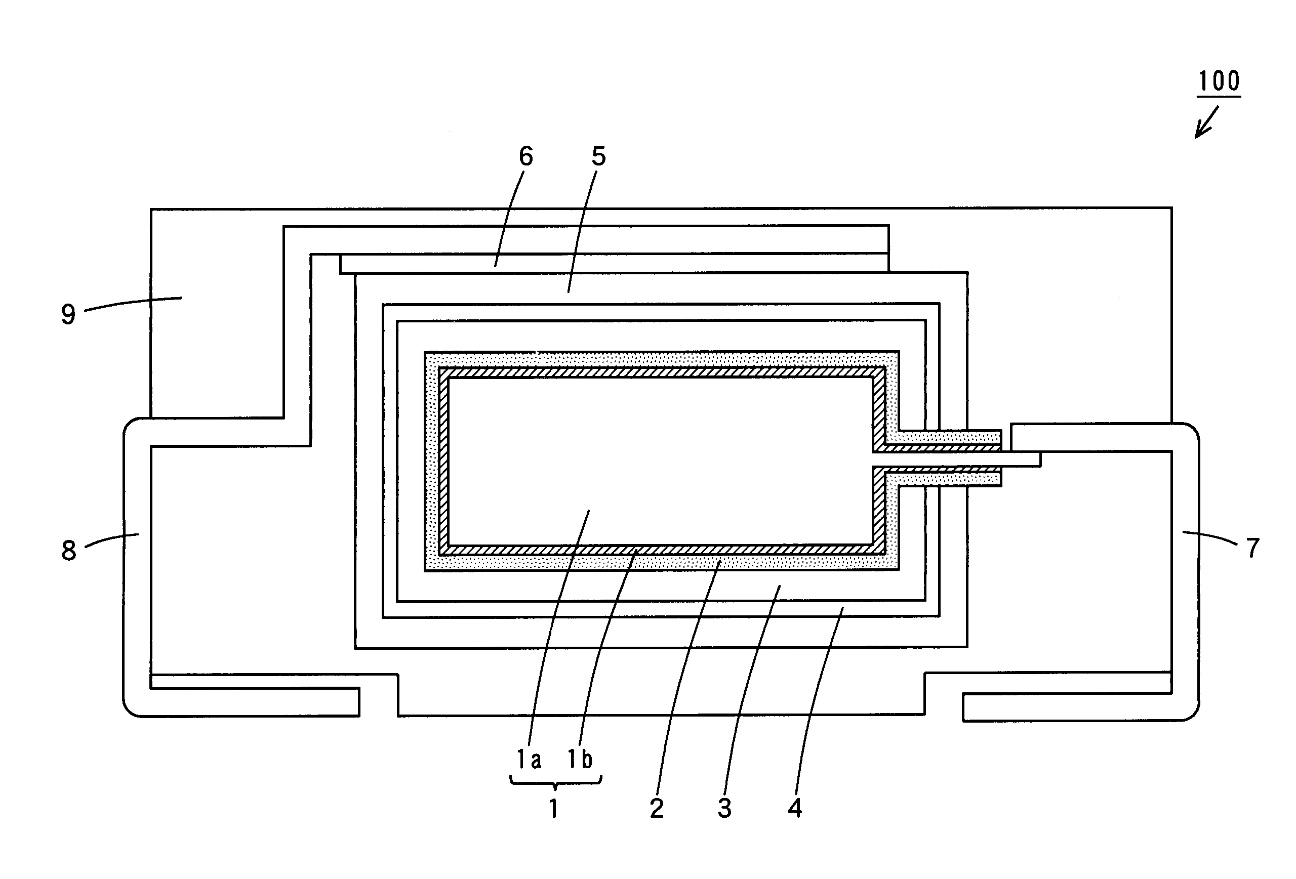
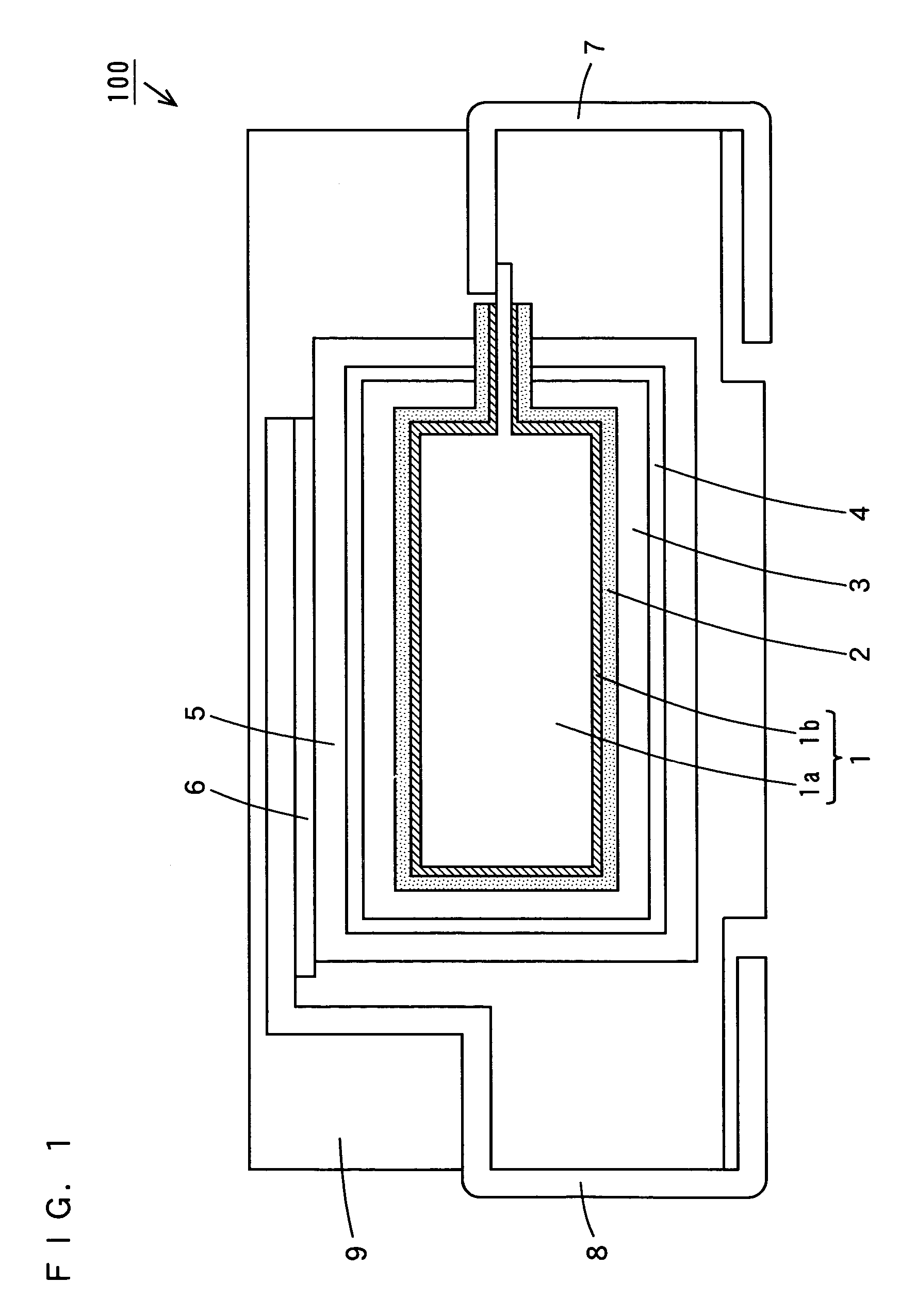
[0063]In Inventive Example 1, a solid electrolytic capacitor as shown in FIG. 3 was prepared by the following method.

[0064](Oxidizing Step 1)

[0065]A niobium film as thick as 0.1 mm was used as a niobium substrate 1a. The niobium substrate 1a was allowed to stand for 30 minutes for oxidization in a 0.5 wt % phosphoric acid aqueous-solution maintained at 60° C. at a constant voltage of 45 V, and a dielectric layer 2 composed of niobium oxide was formed on the surface of the niobium substrate 1a.

[0066](Nitriding Step)

[0067]Now, the niobium substrate 1a having the dielectric layer 2 formed thereon was allowed to stand in an electric furnace maintained at 600° C. and 0.1 atmospheric pressure for five minutes. In this way, a niobium nitride layer 1b was formed between the niobium substrate 1a and the dielectric layer 2.

[0068](Oxidizing Step 2)

[0069]The niobium substrate 1a was oxidized again in a 0.5 wt % phosphoric acid aqueous solution maintained at 60° C. In this wa...

##ventive examples 2 to 15

Inventive Examples 2 to 15

[0090]In Inventive Examples 2 to 15, the correlation between the nitrogen content and leakage current was examined.

[0091]Here, in Inventive Examples 2 to 15, the treatment temperature in the nitriding step in the process of preparing a capacitor in Inventive Example 1 was changed in the range from 120° C. to 1000° C. The treatment temperatures in the nitriding step in Inventive Examples 2 to 15 were 120° C., 200° C., 250° C., 300° C., 600° C., 700° C., 800° C., 850° C., 870° C., 900° C., 920° C., 940° C., 970° C., and 1000° C., respectively. The other conditions were the same as those of Inventive Example 1. Note that the capacitor in Inventive Example 6 was the same as the capacitor prepared in Inventive Example 1.

[0092](Evaluation)

[0093]For the capacitors in Inventive Examples 2 to 15, the nitrogen content, leakage current, and compounds identified by X-ray powder method are given in Table 2.

[0094]Note that the respective the leakage current measurement r...

##ventive example 16

Inventive Example 16

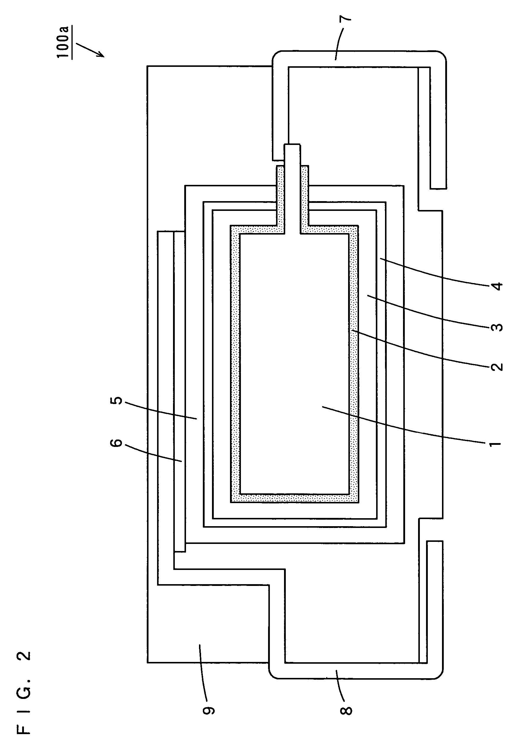
[0101]In Inventive Example 16, a solid electrolytic capacitor shown in FIG. 2 was prepared by the following method.

[0102](Step of Producing Niobium Powder)

[0103]Niobium powder having an average particle size of 1 μm was thermally treated for one hour in a nitrogen atmosphere at 1000° C. and 0.1 atmospheric pressure.

[0104](Step of Producing Niobium Nitride)

[0105]The thermally treated niobium powder was sintered and formed into an anode 1 composed of niobium nitride.

[0106](Oxidizing Step)

[0107]The anode 1 was then oxidized for 10 hours in a 0.5 wt % phosphoric acid aqueous solution maintained at 60° C. at a constant voltage of 10 V, and a dielectric layer 2 composed of niobium oxide was formed on the surface of the anode 1.

[0108](Step of Producing Solid Electrolytic Capacitor)

[0109]The dielectric layer 2 had its surface coated with a conductive polymer layer 3 composed of polypyrrole by electrolytic polymerization. In this case, the conductive polymer layer 3 was f...


PUM

PropertyMeasurementUnit
temperatureaaaaaaaaaa
constant voltageaaaaaaaaaa

Abstract

A solid electrolytic capacitor has an anode composed of a niobium substrate and a niobium nitride layer, and a dielectric layer composed of niobium oxide is formed on the surface of the niobium nitride layer. In the solid electrolytic capacitor, the nitrogen content based on the total weight of the niobium substrate, the niobium nitride layer, and the dielectric layer is preferably not less than 0.001% by weight nor more than 0.2% by weight. In another solid electrolytic capacitor, an anode is formed by sintering thermally treated niobium powder in a nitrogen atmosphere. A dielectric layer composed of niobium oxide is formed on the surface of the anode. In the solid electrolytic capacitor, the composition ratio X of the niobium powder (NbNX) is preferably not less than 0.05 nor more than 1.0.

Description

BACKGROUND OF THE INVENTION[0001]1. Field of the Invention[0002]The present invention relates to a solid electrolytic capacitor and a manufacturing method thereof.[0003]2. Description of the Background Art[0004]Niobium has a dielectric constant about 1.8 times as large as that of tantalum which is a material for conventional solid electrolytic capacitors. Therefore, Niobium has been attracted much attention as a material for next-generation, high capacitance solid electrolytic capacitors.[0005]However, when the solid electrolytic capacitor is subjected to high heat in a reflow soldering step, oxygen in a dielectric layer including niobium oxide is partly diffused into the anode and the thickness of the dielectric layer is reduced. As a result, leakage current is more likely to be caused in the dielectric layer.[0006]In one suggested solid electrolytic capacitor, a niobium nitride region is formed in a niobium oxide layer as a dielectric in order to reduce changes in capacitance caus...

Claims


Application Information

Patent Timeline
Patent Type & Authority Patents(United States)
IPC IPC(8): H01G9/04H01G9/145H01G9/00H01G9/025H01G9/042H01G9/052H01G9/15
CPCH01G9/0032H01G9/0525H01G9/042
Inventor YANO, MUTSUMITAKATANI, KAZUHIROKIMOTO, MAMORU
Owner SANYO ELECTRIC CO LTD
Why Eureka
Try Eureka