

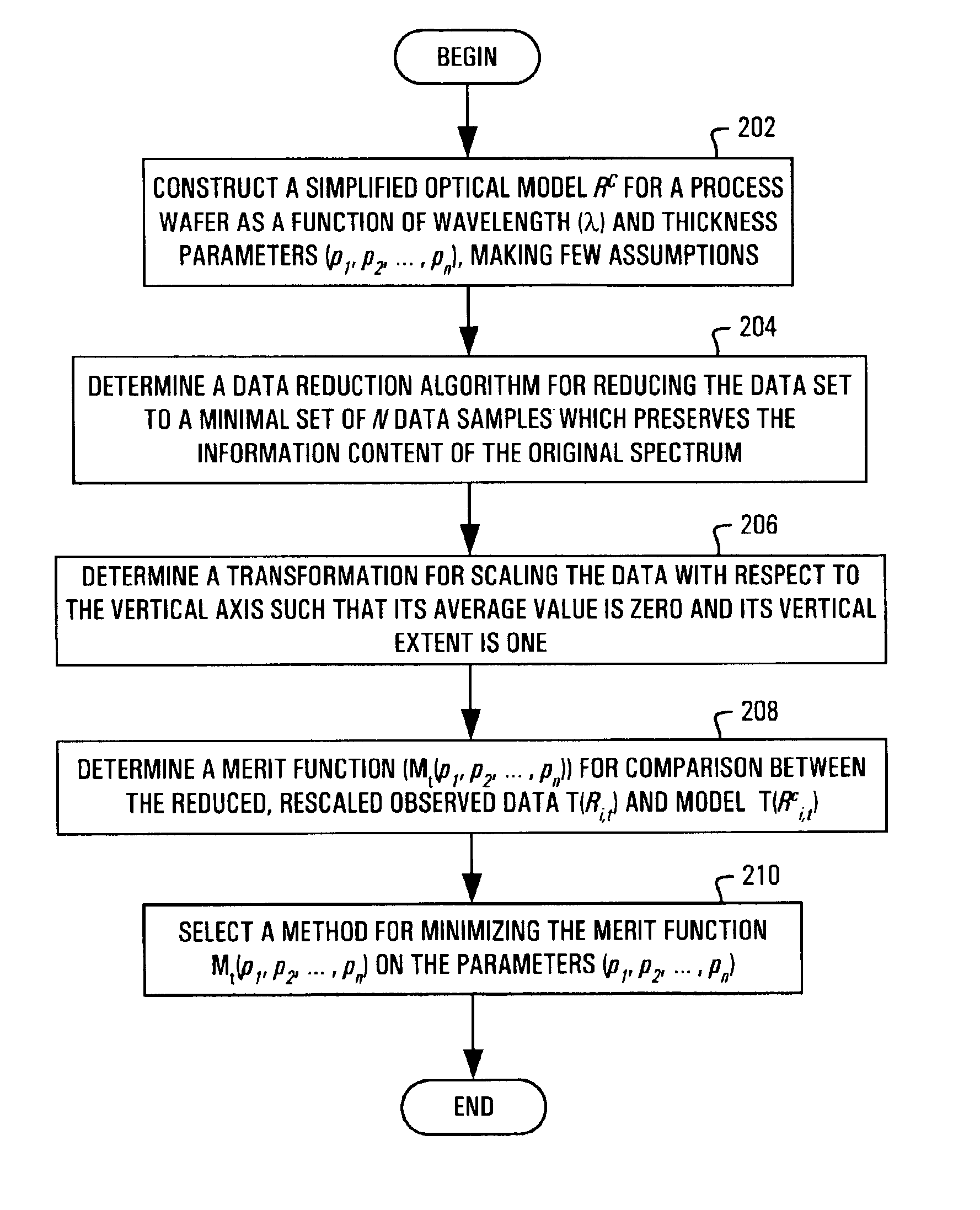
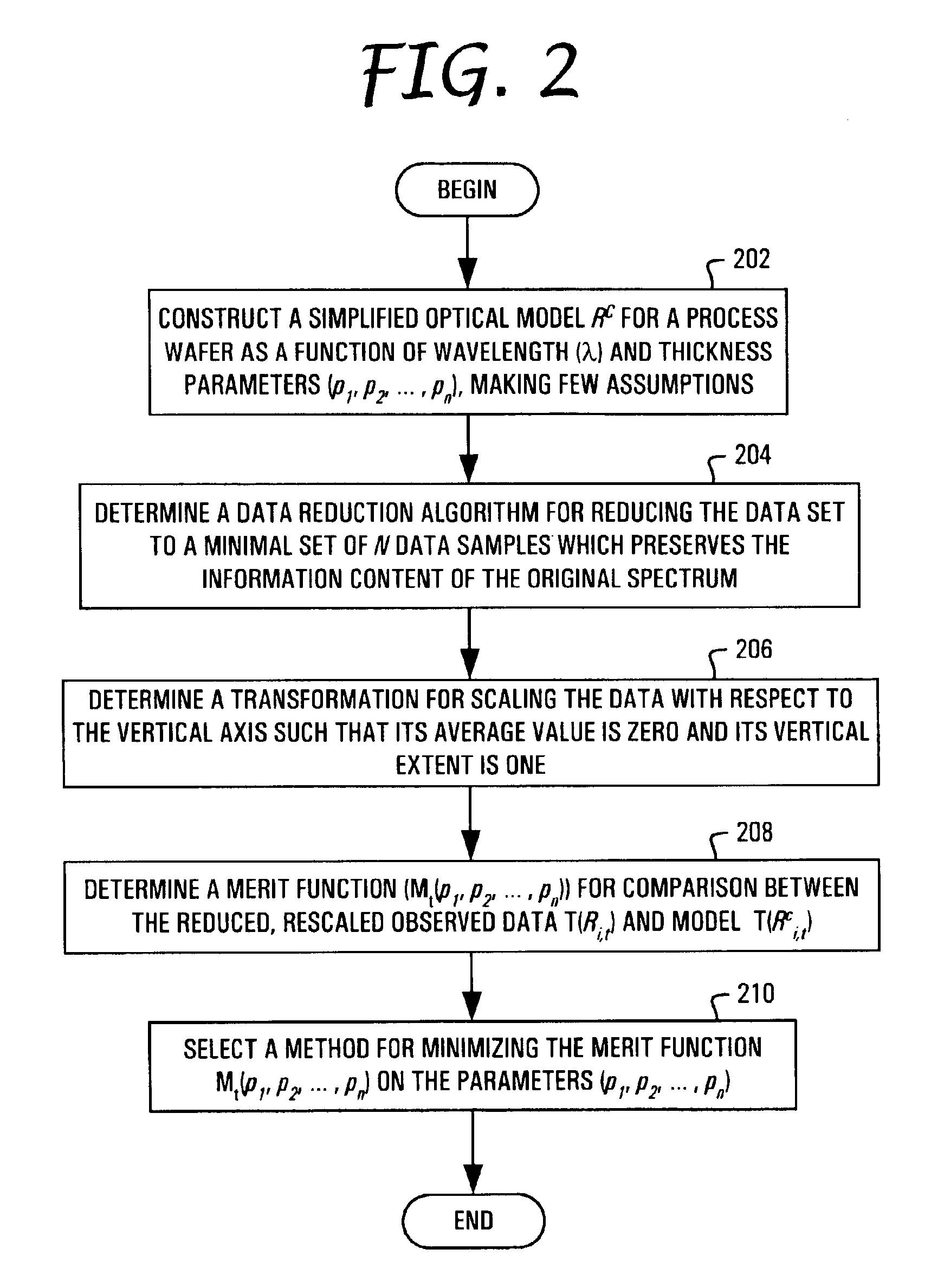
System and method for in-situ monitor and control of film thickness and trench depth
a technology of in-situ monitor and control, applied in the field of semiconductor processing, can solve the problems of inability to perform calibration measurements, material, time and labor, and loss of product, and achieve the effect of reducing the cost of calibration measurement, and reducing the cost of measuremen
- Summary
- Abstract
- Description
- Claims
- Application Information
AI Technical Summary
Benefits of technology
Problems solved by technology
Method used
Image

Examples
Embodiment Construction
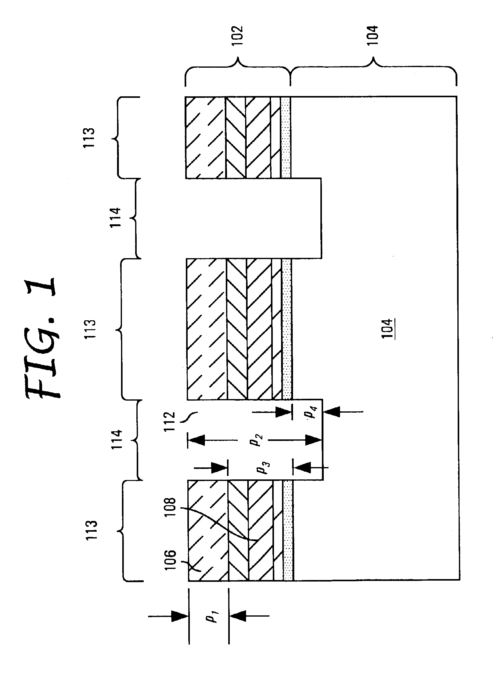
[0053]FIG. 1 is a diagram of a cross-sectional view of an exemplary STI structure. The present STI structure is comprised of two discrete region types; region 113 and region 114. The first type, region 113, is a multilayer dielectric stack 102 on top of a silicon substrate 104. Top layer 106 of the multilayer dielectric stack forming region 102 is photoresist. Below top layer 106 are intermediate layer(s) 108. The thickness of each layer in region 113 is known except for top layer 106 which is not known i.e., the thicknesses of intermediate layer(s) 108 are known. Region 114, the second type of region, is in the exemplary STI structure comprised of substrate 104, since in the depicted exemplary STI structure, trench 112 initially extends through region 108 and to or into region 104.
[0054]Trench 112 is formed as result of a trench excavation process, the type of which is unimportant for the purpose of describing the present invention, but may be any known process such as plasma etchi...
PUM
 Abstract
Description
Claims
Application Information