Simplified process to design integrated circuits

a technology of integrated circuits and design processes, applied in the field of electronic integrated circuit design, can solve the problems of increasing complexity of integrated circuits and chips, increasing the difficulty of specifying and designing chips that perform as actually specified, and achieving the effect of enhancing the design cycl

Active Publication Date: 2006-05-30
BELL SEMICON LLC
View PDF16 Cites 51 Cited by
  • Summary
  • Abstract
  • Description
  • Claims
  • Application Information

AI Technical Summary

Problems solved by technology

Integrated circuits and chips have become increasingly complex, with the speed and capacity of chips doubling about every eighteen months.
An increased density of transistors per square centimeter and faster clock speeds, however, make it increasingly difficult to specify and design a chip that performs as actually specified.
Unanticipated and sometimes subtle interactions between the transistors and other electronic structures may adversely affect the performance of the circuit.
These difficulties increase the expense and risk of designing and fabricating chips, especially those that are custom designed for a specific application.
The demand for complex custom-designed chips increase with the increasing variety of microprocessor-driven applications and products, yet the time and money required to design chips have become a bottleneck in the time it takes to bring these products to market.
Without an assured successful outcome within a specified time, the risks have risen along with costs and the result is that fewer organizations are willing to attempt the design and manufacture of custom chips.
As the software tools evolve, however, the tools themselves have become increasingly complex requiring more time to master and use them.
Correspondingly, the cost of staffing, training, and coordinating the various aspects of chip design has also increased.
Today, however, the software tools used in chip design are so complex that it is difficult to adapt them to this higher level of abstraction.
Coordinating these realms of complexity is a challenge in the design and fabrication of a custom chip.
The utility of these chips is limited by factors such as complexity, cost, time, and design constraints.
FPGAs, however, are very expensive and have the largest die size.
The disadvantage of FPGAs, moreover, is their relatively high cost per function, relatively low speed, and high power consumption.
Programmable gate arrays (PGAs) are also flexible in the numerous possible applications that can be achieved but not quite as flexible as the FPGAs, and are more time-consuming to modify and test.
ASICs, however, are very complex to design and prototype because of their speed and quality.
Application Specific Standard Products (ASSPs) are hard-wired standard chips that meet a specific need, but this customization is both time-consuming and costly.
Documenting, implementing, connecting, and testing these registers and internal memories is extremely time consuming and prone to errors.
This approach is time consuming, tedious, and prone to errors created by manual editing.

Method used


Image

  • Simplified process to design integrated circuits
  • Simplified process to design integrated circuits
  • Simplified process to design integrated circuits

Examples


Embodiment Construction

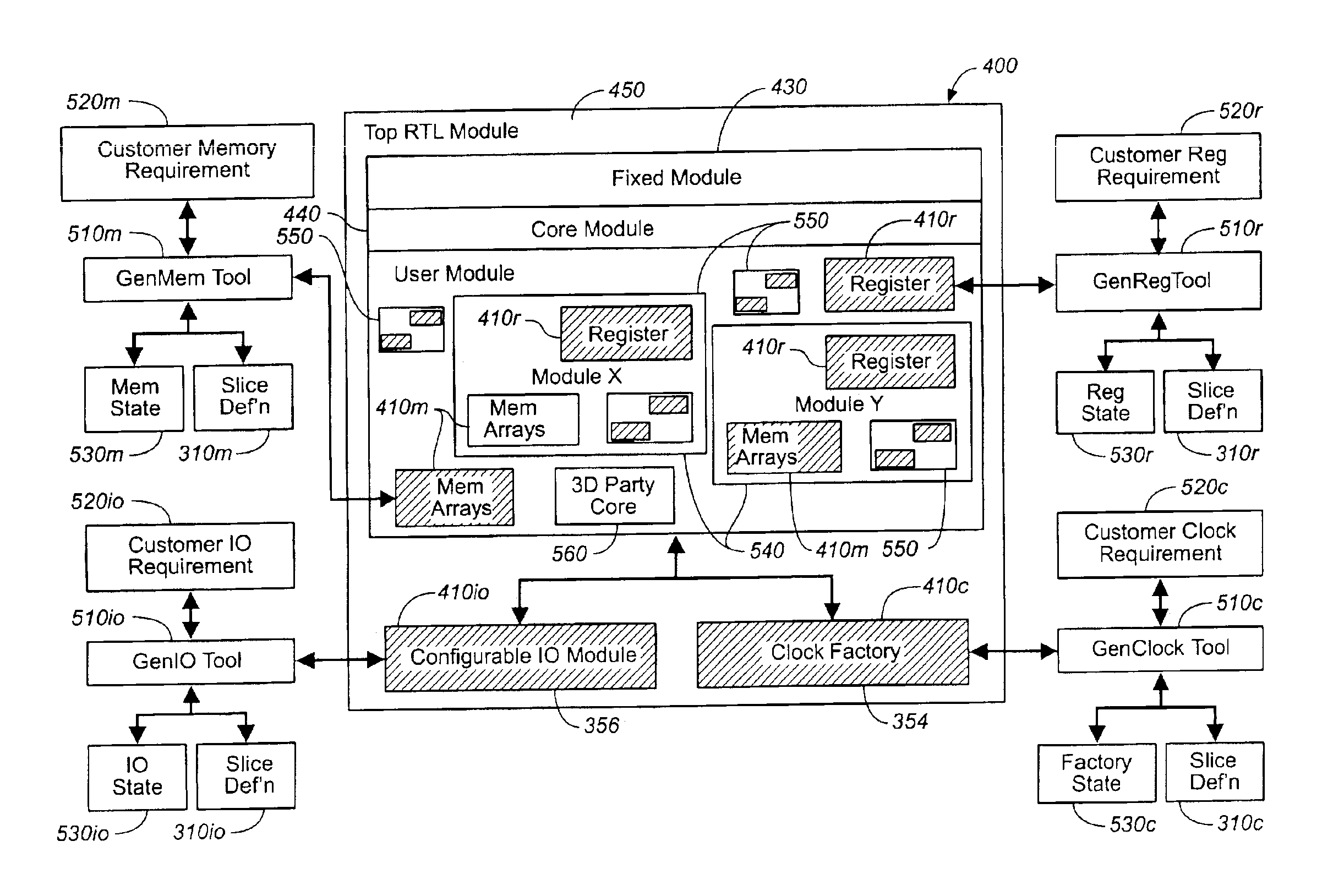
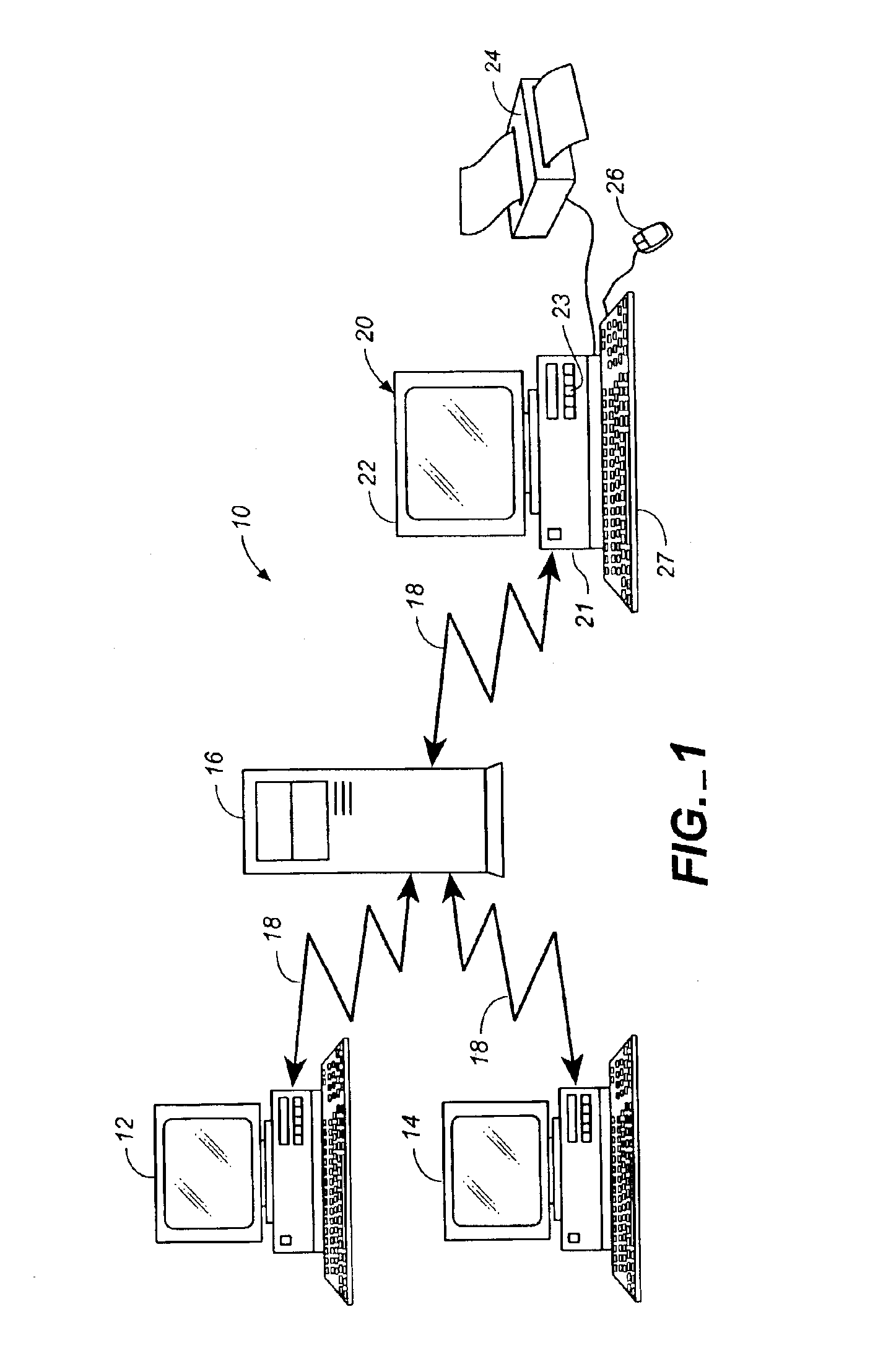
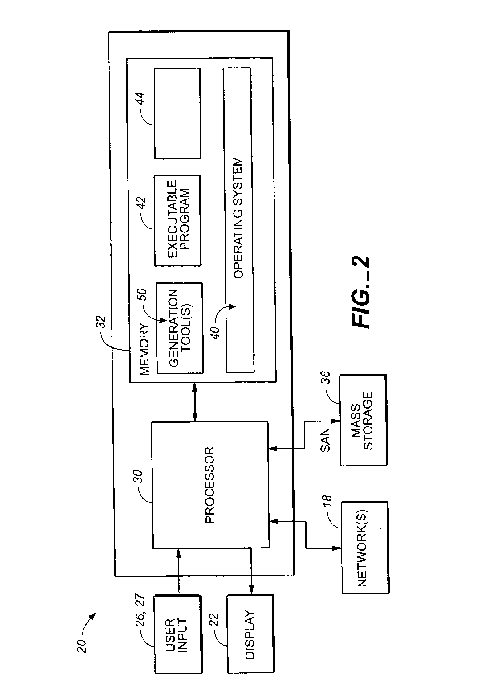
[0021]Referring to the drawings, FIG. 1 illustrates an exemplary computer system 10 upon which the suite of generation tools could be installed and / or used. Computer system 10 is illustrated as a networked computer system that includes one or more client computers 12, 14 and 20 such as workstations coupled through a network 18 to a server 16. Server 16 could also be a personal computer-based server, a minicomputer, a midrange computer, or a mainframe computer. While shown here as a point-to-point connection, computers 12 and 14 need not be coupled to server 16 directly, but may be coupled to yet another network which in turn is connected to server 16. Network 18 may represent practically any type of networked interconnection including but not limited to local-area, wide-area, wireless, and public networks such as the Internet, and any number of routers and hubs connected in between, e.g., a local-area network to a wide-area network to the Internet through a series of routers and / or ...


PUM


Abstract

A set of tools is provided herein that produces useful, proven, and correct integrated semiconductor chips. Having as input either a customer's requirements for a chip, or a design specification for a partially manufactured semiconductor chip, the tools generate the RTL for control plane interconnect; memory composition, test, and manufacture; embedded logic analysis, trace interconnection, and utilization of spare resources on the chip; I / O qualification, JTAG, boundary scan, and SSO analysis; testable clock generation, control, and distribution; interconnection of all of the shared logic in a testable manner from a transistor fabric and / or configurable blocks in the slice. The input customer requirements are first conditioned by RTL analysis tools to quickly implement its logic. The slice definition and the RTL shell provides the correct logic for a set of logic interfaces for the design specification to connect. The tools share a common database so that logical interactions do not require multiple entries. The designs are qualified, tested, and verified by other tools. The tools further optimize the placement and timing of the blocks on the chip with respect to each other and with respect to placement on a board. The suite may be run as batch processes or can be driven interactively through a common graphical user interface. The tools also have an iterative mode and a global mode. In the iterative mode, one or more of the selected tools can generate the blocks or modify a design incrementally and then look at the consequences of the addition, or change. In the global mode, the semiconductor product is designed all at once in a batch process as above and then optimized altogether. This suite of generation tools generates design views including a qualified netlist for a foundry to manufacture.

Description

CROSS REFERENCE TO RELATED APPLICATIONS[0001]The present application is related to the following United States patent applications, which are hereby incorporated by reference in their entireties: copending application Ser. No. 10 / 435,168 entitled Automation of the Development, Testing and Release of a Flow Framework and Methodology to Design Integrated Circuits; copending application Ser. No. 10 / 318,792 entitled Flexible Template Having Embedded Gate Array and Composable Memory for Integrated Circuits, filed Dec. 13, 2002; copending application Ser. No. 10 / 318,623 entitled Automated Selection and Placement of the Memory During Design of an Integrated Circuit, filed Dec. 13, 2002; copending application Ser. No. 10 / 334,568 entitled Configurable Input / Output Buffer Structures During Design of Integrated Circuits, now U.S Pat. No. 6,823,502; copending application Ser. No. 10 / 465,186 entitled Design and Testing the Interconnection of Addressable Devices of Integrated Circuits; copending ...

Claims


Application Information

Patent Timeline
Patent Type & Authority Patents(United States)
IPC IPC(8): G06F17/50G06F9/455
CPCG06F17/505G06F30/327
Inventor BROBERG, III, ROBERT NEAL CARLTONBYRN, JONATHAN WILLIAMDELP, GARY SCOTTENEBOE, MICHAEL K.MCCLANNAHAN, GARY PAULNATION, GEORGE WAYNEREULAND, PAUL GARYSANDOVAL, THOMASWINGREN, MATTHEW SCOTT
Owner BELL SEMICON LLC
Why Eureka
Try Eureka