Fabrication method of semiconductor device

a technology of semiconductor devices and fabrication methods, which is applied in the direction of polycrystalline material growth, crystal growth process, chemically reactive gases, etc., can solve the problems of difficult to obtain the required crystallinity, difficult to obtain a good annealing effect across the wide area, and the irradiation of laser light is apt to become unstable, so as to achieve high crystallinity and low concentration of metal elements.

Inactive Publication Date: 2006-06-06
SEMICON ENERGY LAB CO LTD
View PDF274 Cites 79 Cited by
  • Summary
  • Abstract
  • Description
  • Claims
  • Application Information

AI Technical Summary

Benefits of technology

[0033]As a result of the heat treatment for gettering, a thermal oxide film containing the nickel element in high concentration is formed. Then, the crystal silicon film having the high crystallinity and having low concentration of the metal element may be obtained by eliminating this thermal oxide film.

Problems solved by technology

However, it has been the fact that it is difficult to obtain a required crystallinity across the wide area through the heat treatment because it may cause nonuniformity in the crystallization.
Further, although it is possible to obtain the high crystallinity partly by irradiating laser light, it is difficult to obtain a good annealing effect across the wide area.
In particular, the irradiation of the laser light is apt to become unstable under the condition for obtaining the good crystallinity.
However, it is difficult to obtain a crystal silicon film having a high crystallinity and homogeneity across a large area which is required for an active matrix type liquid crystal display.
Further, because the metal element is contained within the film and an amount thereof to be introduced has to be controlled very carefully, there is a problem in its reproducibility and stability (electrical stability of a device obtained).
Further, there is a problem that an elapsed change of the characteristics of a semiconductor device to be obtained is large or an OFF value, in case of a thin film transistor, is large, for example due to the influence of the remaining metal element.
That is, although the metal element which promotes the crystallization of silicon plays the useful role in obtaining the crystal silicon film, its existence becomes a minus factor which causes various problems after obtaining the crystal silicon film once.

Method used


Image

  • Fabrication method of semiconductor device
  • Fabrication method of semiconductor device
  • Fabrication method of semiconductor device

Examples


first embodiment

[0041]An arrangement for obtaining a crystal silicon film on a glass substrate by utilizing nickel element will be explained in the present embodiment.

[0042]At first, the crystal silicon film having a high crystallinity is obtained by an action of nickel element in the present embodiment.

[0043]Then, laser light is irradiated to enhance the crystallinity of the film and to diffuse nickel element existing locally concentratedly within the film. That is, the block of nickel is extinguished.

[0044]Next, a thermal oxide film is formed on the crystal silicon film by thermal oxidation. At this time, the nickel element remaining in the crystal silicon film thus obtained is gettered to the thermal oxide film. Because the nickel element is distributed by the irradiation of the laser light, the gettering proceeds effectively.

[0045]Then, the thermal oxide film containing the nickel element in high concentration as a result of the gettering is eliminated. Thereby, the crystal silicon film having ...

second embodiment

[0094]The present embodiment relates to a case when Cu is used as the metal element which promotes the crystallization of silicon in the arrangement shown in the first embodiment. In this case, cupric acetate [Cu(CH3 COO)2] or cupricchloride (CuCl22H2O) may be used as the solution for introducing Cu.

third embodiment

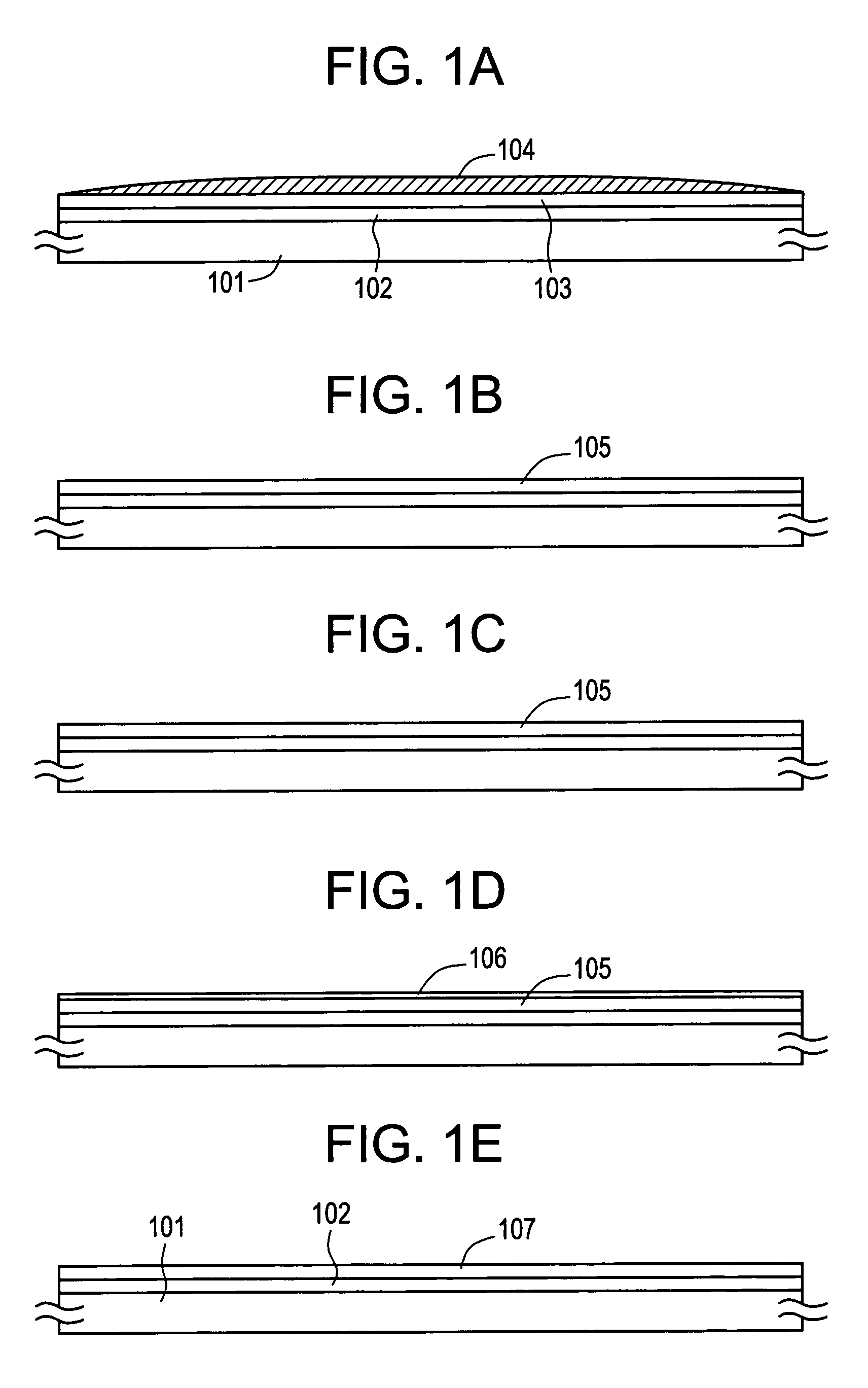
[0095]The present embodiment relates to a case of growing crystal in the form different from that in the first embodiment. That is, the present embodiment relates to a method of growing the crystal in a direction parallel to the substrate, i.e. a method called lateral growth, by utilizing the metal element which promotes crystallization of silicon.

[0096]FIG. 2 shows the fabrication process according to the present embodiment. At first, a silicon oxide nitride film is formed as an underlying film 202 in a thickness of 3000 angstrom on the Corning 1737 glass substrate (or a quartz substrate) 201.

[0097]Next, an amorphous silicon film 203 which is the starting film of a crystal silicon film is formed in a thickness of 600 angstrom by reduced pressure thermal CVD. The thickness of the amorphous silicon film is preferable to be less than 2000 angstrom as described before.

[0098]It is noted that plasma CVD may be used instead of the reduced pressure thermal CVD.

[0099]Next, a silicon oxide f...


PUM

PropertyMeasurementUnit
temperatureaaaaaaaaaa
angleaaaaaaaaaa

Abstract

Concentration of metal element which promotes crystallization of silicon and which exists within a crystal silicon film obtained by utilizing the metal element is reduced. A first heat treatment for crystallization is implemented after introducing nickel to an amorphous silicon film 103. Then, laser light is irradiated to diffuse the nickel element concentrated locally. After that, another heat treatment is implemented within an oxidizing atmosphere at a temperature higher than that of the previous heat treatment. A thermal oxide film 106 is formed in this step. At this time, the nickel element is gettered to the thermal oxide film 106. Then, the thermal oxide film 106 is removed. Thereby, a crystal silicon film 107 having low concentration of the metal element and a high crystallinity can be obtained.

Description

FIELD OF THE INVENTION[0001]The present invention relates to a semiconductor device typified by a thin film transistor and to a fabrication method thereof. Specifically, the present invention relates to a semiconductor device using a crystalline silicon thin film formed on a glass substrate or a quartz substrate and to a fabrication method thereof.DESCRIPTION OF RELATED ART[0002]Hitherto, there has been known a thin film transistor using a silicon film, i.e. a technology for forming the thin film transistor by using the silicon film formed on a glass substrate or quartz substrate.[0003]The glass substrate or quartz substrate is used because the thin film transistor is used for an active matrix type liquid crystal display. While a thin film transistor has been formed by using an amorphous silicon film in the past, it is being tried to fabricate the thin film transistor by utilizing a silicon film having a crystallinity (referred to as “crystalline silicon film” hereinbelow) in order ...

Claims


Application Information

Patent Timeline
Patent Type & Authority Patents(United States)
IPC IPC(8): C30B23/00
CPCH01L21/02488H01L21/02532H01L21/02672H01L27/1277H01L21/3221H01L27/12H01L21/02675
Inventor YAMAZAKI, SHUNPEITERAMOTO, SATOSHIKOYAMA, JUNOGATA, YASUSHIHAYAKAWA, MASAHIKOOSAME, MITSUAKI
Owner SEMICON ENERGY LAB CO LTD
Why Eureka
Try Eureka