Method of forming interlayer insulating film

a technology of interlayer insulating film and film layer, which is applied in the direction of coating, chemical vapor deposition coating, plasma technique, etc., can solve the problems of fatal failure, difficult to use silicon oxide film, and degradation of lsi performance, so as to improve the heat resistance of the interlayer insulating film, improve the formability, and improve the heat resistance. the effect of the film

Inactive Publication Date: 2006-06-13
PANASONIC CORP
View PDF45 Cites 35 Cited by
  • Summary
  • Abstract
  • Description
  • Claims
  • Application Information

AI Technical Summary

Benefits of technology

[0021]In view of the foregoing, a first object of the present invention is to improve the film formability, cost efficiency, and processability of an interlayer insulating film composed of an organic SOG film. A second object of the present invention is to improve the heat resistance of an interlayer insulating film composed of an organic polymer film.

Problems solved by technology

With the increasing miniaturization of an LSI formed on a semiconductor substrate, wiring capacitance which is parasitic capacitance between metal wires has remarkably increased, while degraded performance of the LSI due to a wiring delay caused thereby has presented a serious problem.
If an interlayer insulating film with low heat resistance is used, a thermal treatment at about 400° C. performed in a semiconductor manufacturing process will soften the interlayer insulating film and undulate wiring, which may cause a fatal failure such as a disconnection or short circuit.
Hence, it is difficult to use silicon oxide films including the fluorine-doped silicon oxide film as interlayer insulating films in an extremely miniaturized LSI.
However, since the foregoing organic SOG film is formed by repeatedly performing the steps of applying the organic SOG agent and thermally curing the applied organic SOG agent several times, it has the disadvantages of poor film formability resulting from a large amount of time required by the formation of the organic SOG film and high cost resulting from the major portion of the agent wasted during the spin coating.
The resulting H2O causes the oxidization and contamination of the metal forming the contacts, leading to faulty conduction at a contact.
As for the organic polymer film composed of the fluorinated amorphous carbon film, it has the advantage of an extremely low dielectric constant over the organic SOG film but is inferior thereto in heat resistance because of its low glass transition temperature.

Method used


Image

  • Method of forming interlayer insulating film
  • Method of forming interlayer insulating film
  • Method of forming interlayer insulating film

Examples


first embodiment

[0066]An interlayer insulating film according to a first embodiment is a plasma polymerization film formed by inducing plasma polymerization of a material containing, as a main component, phenyltrimethoxysilane which is an organic silicon compound represented by the following general formula:

R1xSi(OR2)4-x

(where R1 is a phenyl group or a vinyl group; R2 is an alkyl group; and x is an integer of 1 to 3).

[0067]A description will be given to a method of forming the interlayer insulating film according to the first embodiment.

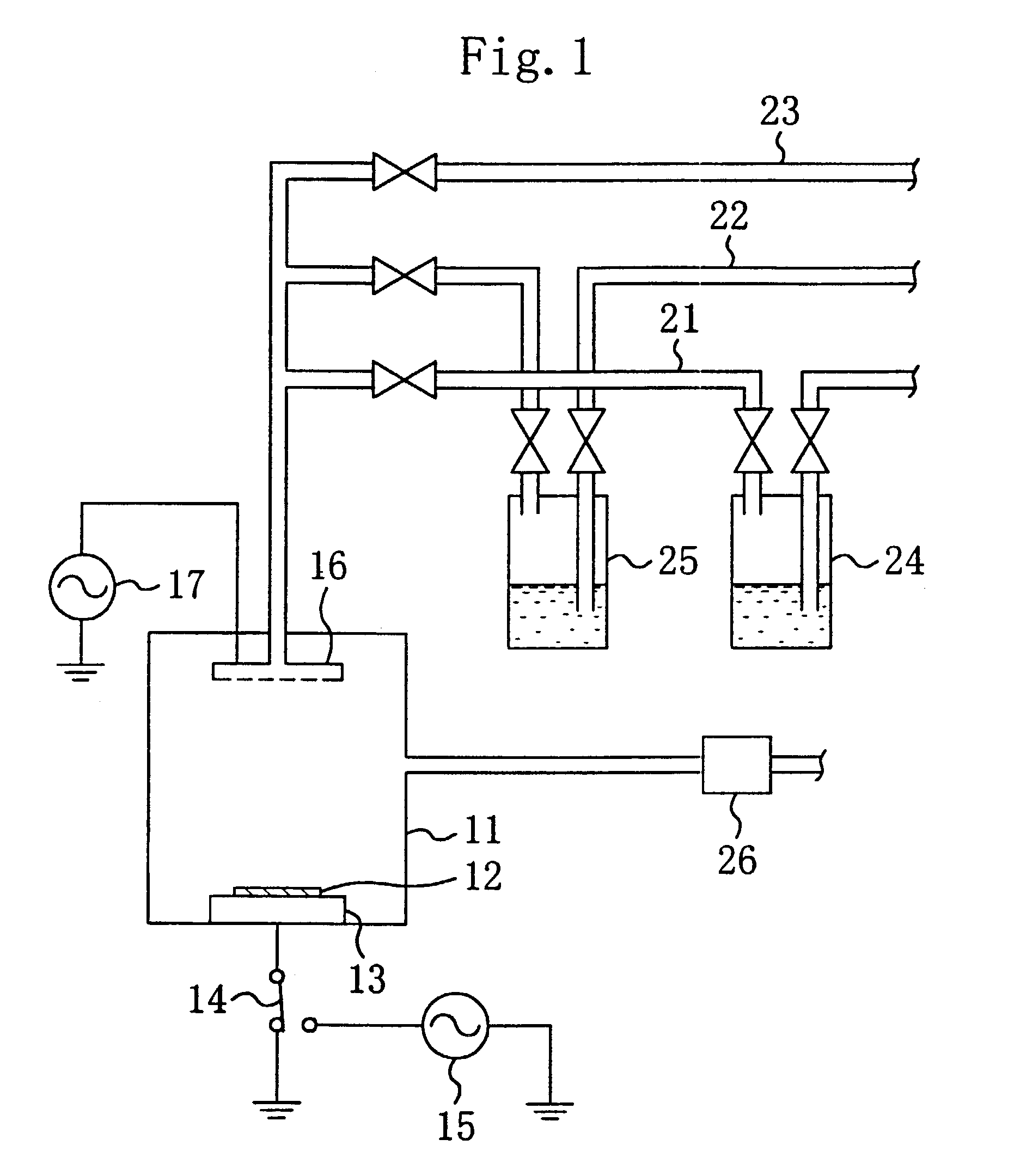
[0068]First, the semiconductor substrate 12 is placed on the sample stage 13 heated to, e.g., 400° C. and grounded by the change-over switch 14 and then the reaction chamber 11 is evacuated by the vacuum pump 26.

[0069]Next, phenyltrimethoxysilane represented by the following Chemical Formula 1:

[0070]

is contained in the first container 24, while carrier gas composed of, e.g., argon is supplied at a flow rate of 480 cc / min to the first container 24 so that bubbled phe...

second embodiment

[0085]An interlayer insulating film according to a second embodiment is a fluorinated amorphous carbon film formed by inducing plasma polymerization of a material having, as a main component, 1,1,1,3,3-pentafluorpropene which is a fluorinated carbon compound having a double bond of carbon atoms in a molecule thereof and containing a hydrogen atom.

[0086]A description will be given to a method of forming the interlayer insulating film according to the second embodiment.

[0087]First, the semiconductor substrate 12 is placed on the sample stage 13 grounded by the change-over switch 14 and then the reaction chamber 11 is evacuated by the vacuum pump 26 .

[0088]Next, 1,1,1,3,3-pentafluoropropene is contained in the first container 24, while carrier gas composed of, e.g., argon is supplied at a flow rate of 50 to 500 sccm to the first container 24 so that bubbled 1,1,1,3,3-pentafluoropropene is introduced into the reaction chamber 11.

[0089]After the pressure inside the reaction chamber 11 is...

third embodiment

[0097]An interlayer insulating film according to a third embodiment is a fluorinated amorphous carbon film formed by inducing plasma polymerization of a material having, as a main component, hexafluoropropene which is a fluorinated carbon compound having a double bond of carbon atoms in a molecule thereof and containing no hydrogen atom.

[0098]Since the third embodiment has been implemented by replacing the material used in the second embodiment, a description will be given only to the material.

[0099]When hexafluoropropene is introduced into the reaction chamber 11, it is partially decomposed and changed into a plasma, while monomers, ions, and radicals are generated as decomposition products and polymerized to form the interlayer insulating film composed of the plasma polymerization film on the semiconductor substrate 12.

[0100]Since hexafluoropropene according to the third embodiment contains no hydrogen atom, the resulting interlayer insulating film was a fluorinated amorphous carb...


PUM

PropertyMeasurementUnit
heat resistanceaaaaaaaaaa
dielectric constantaaaaaaaaaa

Abstract

A material containing, as a main component, an organic silicon compound represented by the following general formula:
R1xSi(OR2)4-x
(where R1 is a phenyl group or a vinyl group; R2 is an alkyl group; and x is an integer of 1 to 3) is caused to undergo plasma polymerization or react with an oxidizing agent to form an interlayer insulating film composed of a silicon oxide film containing an organic component. As the organic silicon compound where R1 is a phenyl group, there can be listed phenyltrimethoxysilane or diphenyldimethoxysilane. As the organic silicon compound where R1 is a vinyl group, there can be listed vinyltrimethoxysilane or divinyldimethoxysilane.

Description

[0001]This application is a divisional of application Ser. No. 09 / 900,142, filed Jul. 9, 2001 now U.S. Pat. No. 6,558,756, which is a divisional of application Ser. No. 09 / 365,509, filed Aug. 2, 1999, now abandoned, which is a divisional of application Ser. No. 08 / 919,271, filed Aug. 28, 1997, now U.S. Pat. No. 5,989,998.BACKGROUND OF THE INVENTION[0002]The present invention relates to a method of forming an interlayer insulating film in a semiconductor device.[0003]Known interlayer insulating films formed in semiconductor devices include a silicon oxide film, a silicon oxide film composed of an organic SOG (Spin-On-Glass) containing an organic component, and an organic polymer film.[0004]In general, an interlayer insulating film formed in a semiconductor device is required to have a sufficiently low dielectric constant to achieve lower wiring capacitance and sufficiently high heat resistance to withstand a semiconductor manufacturing process.[0005]With the increasing miniaturizatio...

Claims


Application Information

Patent Timeline
Patent Type & Authority Patents(United States)
IPC IPC(8): C23C16/30C23C16/40C23C16/42C23C16/509H01L21/473C23C16/26H01L21/3105H01L21/312H01L21/314H01L21/316H01L21/768
CPCC23C16/26H01L21/76807C23C16/401H01L21/0212H01L21/02126H01L21/02131H01L21/02205H01L21/02211H01L21/02214H01L21/02216H01L21/02274H01L21/3122H01L21/3127H01L21/314H01L21/31608H01L21/31612H01L21/31629H01L21/31633H01L21/76801C23C16/30H01L21/31051H01L21/31058
Inventor SUGAHARA, GAKUAOI, NOBUOARAI, KOJISAWADA, KAZUYUKI
Owner PANASONIC CORP
Why Eureka
Try Eureka