Adhesive composition, method for preparing the same, adhesive film using the same, substrate for carrying semiconductor and semiconductor device
a technology of adhesive composition and adhesive film, which is applied in the direction of heat-activated film/foil adhesive, film/foil adhesive without carrier, paper/cardboard articles, etc., and can solve the problems of lowering interconnection reliability, lowering interconnection reliability, and increasing cos
- Summary
- Abstract
- Description
- Claims
- Application Information
AI Technical Summary
Benefits of technology
Problems solved by technology
Method used
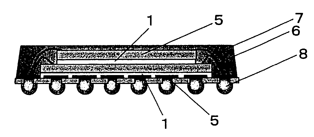
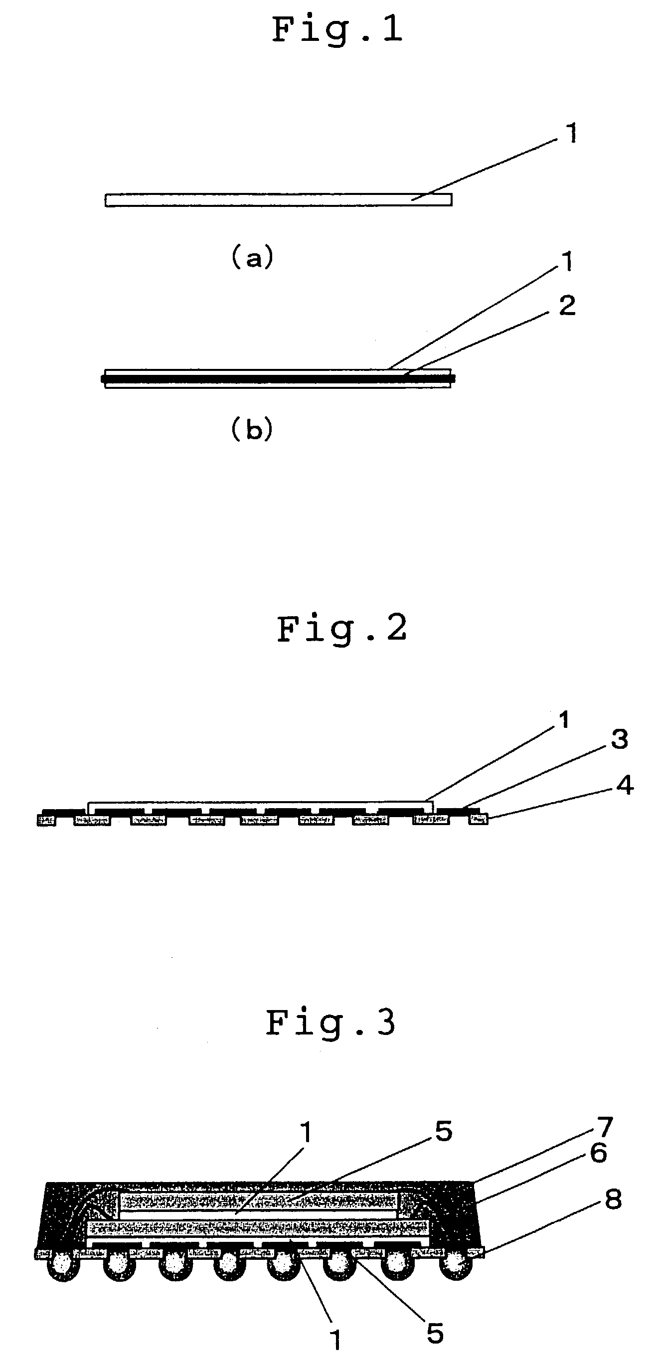
Image

Examples
example 1
Sample 1
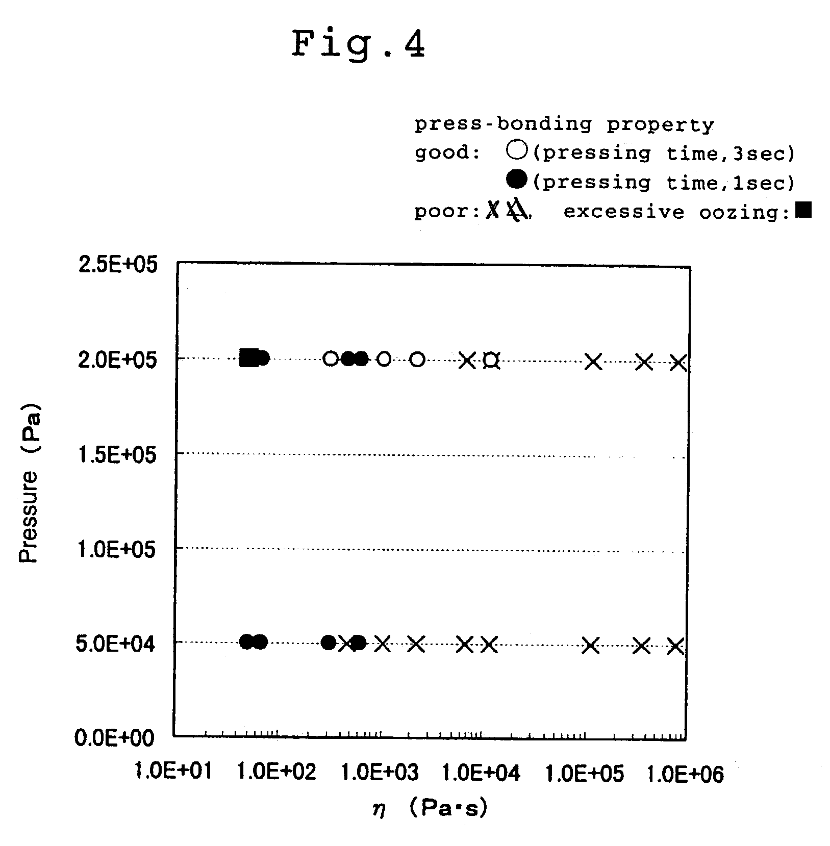
[0183]Methyl ethyl ketone was added to an adhesive composition comprising 45 parts by weight of bisphenol A type epoxy resin (epoxy equivalent 175, manufactured by Tohto Kasei Co., Ltd., trade name: YD-8125) and 15 parts by weight of a cresol novolak type epoxy resin: (epoxy equivalent 210, manufactured by Tohto Kasei Co., Ltd., trade name: YDCN-703) as an epoxy resin, 40 parts by weight of a phenol novolak resin (manufactured by Dainippon Ink & Chemicals, Inc., trade name: Plyofen LF2882) as an epoxy resin curing agent, 66 parts by weight of an epoxy group-containing acrylic rubber as an epoxy group-containing acrylic type copolymer (molecular weight: 1,000,000, grycidyl group-containing repeating unit 3% by weight, Tg: −7° C., manufactured by Teikoku Chemical Industries Co., Ltd.; trade name: HTR-860P-3DR(C)) as a polymer, and, as a curing accelerator, 0.5 part by weight of an imidazole type curing accelerator (manufactured by Shikoku Kasei Kogyo Co., trade name: Curezol 2...
example 2
Sample 7
(1) Preparation of the First Adhesive Layer
[0201]Methyl ethyl ketone was added to an adhesive composition comprising 45 parts by weight of bisphenol A type epoxy resin (epoxy equivalent 175, manufactured by Tohto Kasei Co., Ltd., trade name: YD-8125) and 15 parts by weight of a cresol novolak epoxy resin (epoxy equivalent 210, manufactured by Tohto Kasei Co., Ltd., trade name: YDCN-703) as an epoxy resin, 40 parts by weight of a phenol novolak resin (manufactured by Dainippon Ink & Chemicals, Inc., trade name: Plyofen LF2882) as an epoxy resin curing agent, 66 parts by weight of an epoxy group-containing acrylic rubber as an epoxy group-containing acrylic type polymer (molecular weight: 1,000,000, grycidyl group-containing repeating unit 3% by weight, Tg: −7° C., manufactured by Teikoku Chemical Industries Co., Ltd.; trade name: HTR-860P-3DR(C)) as a polymer, and, as a curing accelerator, 0.5 part by weight of an imidazole type curing accelerator (manufactured by Shikoku Kas...
example 3
Sample 9
[0212]Cyclohexanone was added to an adhesive composition comprising 55 parts by weight of a cresol novolak type epoxy resin with an epoxy equivalent of 210 (manufactured by Tohto Kasei Co., Ltd., trade name: YDCN-703) as an epoxy resin, 45 parts by weight of a phenol resin with a hydroxy group equivalent of 175, moisture absorption of 1.8%, and weight loss by heating at 350° C. of 4% (manufactured by Mitsui Kagaku Kogyo Co., trade name: MILEX XLC-LL) as an epoxy resin curing agent, 1.7 parts by weight of 3-mercaptopropyltrimethoxy silane (manufactured by Nihon Yunicar Co., tradename: NUCA-189) and 3.2 parts by weight of 3-ureidopropyltriethoxy silane (manufactured by Nihon Yunicar Co. Ltd., tradename: NUCA-1160) as a silane coupling agent, and 10 parts by weight of fumed silica with an average particle diameter of 0.016 μm (manufactured by Nippon Aerosil Co., Ltd., trade name: Aerosil R972). The mixture was stirred and then, it was further kneaded using a beads mill for 90 m...
PUM
| Property | Measurement | Unit |
|---|---|---|
| softening point | aaaaa | aaaaa |
| melt viscosity | aaaaa | aaaaa |
| glass transition temperature | aaaaa | aaaaa |
Abstract
Description
Claims
Application Information
 - R&D
- Intellectual Property
- Life Sciences
- Materials
- Tech Scout
- Unparalleled Data Quality
- Higher Quality Content
- 60% Fewer Hallucinations
Browse by: Latest US Patents, China's latest patents, Technical Efficacy Thesaurus, Application Domain, Technology Topic, Popular Technical Reports.
© 2025 PatSnap. All rights reserved.Legal|Privacy policy|Modern Slavery Act Transparency Statement|Sitemap|About US| Contact US: help@patsnap.com