

Method of manufacturing a semiconductor device
a manufacturing method and semiconductor technology, applied in semiconductor devices, instruments, electrical devices, etc., can solve the problems of low dopant species ratio in the resultant plasma, long dose period, etc., and achieve excellent tft characteristics and reduce variations of respective tft characteristics
- Summary
- Abstract
- Description
- Claims
- Application Information
AI Technical Summary
Benefits of technology
Problems solved by technology
Method used
Image

Examples
embodiment 1
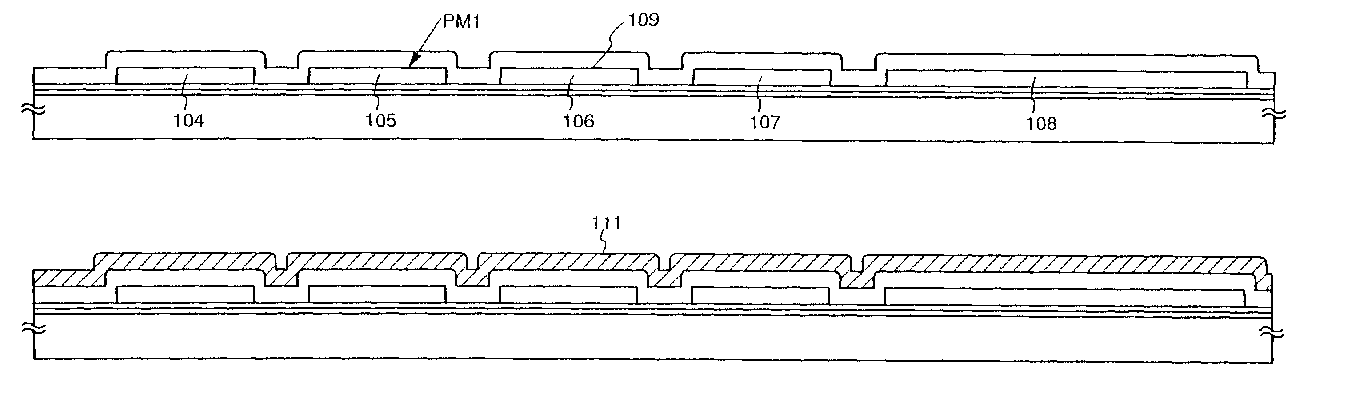
[0089]One of embodiments of the present invention will be described with reference to FIGS. 4A to 4D, 5A to 5C, 6A, and 6B. In particular, a method for simultaneously forming a pixel TFT and a retaining capacitance in a pixel portion as well as a TFT in a driver circuit to be disposed in the peripheral portion of the pixel portion will be described in detail.
[0090]In FIG. 4A, as a substrate 101, a glass substrate made of, e.g., barium borosilicate glass, aluminum borosilicate glass, such as a #7059 glass or a #1737 glass available from Corning, may be used. Alternatively, a quartz substrate may be used as the substrate 101. In the case where the glass substrate is employed, the substrate 101 may be heat treated in advance at a temperature lower than the glass deformation temperature by about 10 to 20° C. Then, an underlying film 102 made of an insulating film such as a silicon oxide film, a silicon nitride film, or a silicon oxynitride film is formed on a surface of the substrate 10...
embodiment 2
[0132]In Embodiment 1, heat-resistive conductive materials such as W or Ta are used for forming the gate electrode. The reason why those materials are used is as follows. The impurity elements added into the semiconductor layer for the purpose of controlling the conductivity type after forming the gate electrode are required to be activated through the thermal annealing at the temperature of 400 to 700° C. Accordingly, the gate electrode is required to have sufficient heat-resisting capability. However, such heat-resistive conductive materials have a large area resistance of about 10 Ω, and therefore, are not necessarily suitable for display devices having a display size of the 4-inch class or more. When a gate line to be connected to the gate electrode is formed of the same material, a line length extending on the substrate is inevitably lengthened. Thus, the disadvantage of wiring delays due to the adverse influence of wiring resistance cannot be ignored.
[0133]For example, in the ...
embodiment 3
[0138]The active matrix substrate can be applied to a reflection-type display device without significant modification. On the other hand, when a transparent-type liquid crystal display device is to be fabricated, the pixel electrode to be provided in each of the pixels in the pixel portion is formed by employing a transparent electrode. In the present embodiment, a method of manufacturing the active matrix substrate for the transparent-type liquid crystal display device will be described with reference to FIGS. 11A through 11D.
[0139]An active matrix substrate is formed in the manner similar to Embodiment 1. In FIG. 11A, the source wirings and the drain wirings are provided by forming a conductive metal film with a sputtering method or a vacuum deposition method. The structure will be described with reference to FIG. 11B in detail by taking the drain wirings 256 as an example. A Ti film 256a having a thickness of 50 to 150 nm is formed to be in contact with the semiconductor film in ...
PUM
 Abstract
Description
Claims
Application Information