During each semiconductor fabrication process, defects such as
particulate contamination and pattern defects may be introduced into the semiconductor devices.
For example, randomly placed defects may be caused by events such as an unexpected increase in
particulate contamination in a manufacturing environment or an unexpected increase in
contamination in process chemicals that are used in fabrication.
Because fabrication of a semiconductor device is composed of many complex process steps, the effects of defects on the total yield typically increase exponentially if an error that is caused by a defect is propagated throughout an entire semiconductor device.
For example, one kind of defect type includes those resulting from
resist or developer problems such as lifting resist, thin resist, extra
photoresist coverage, incomplete or missing resist which may be caused by clogged dispense nozzles or an incorrect process sequence, and developer or water spots.
With the exception of non-uniform or incomplete EBR, such defects generally occur randomly or systematically from lot-to-lot or from
wafer-to-wafer.
There are, however, several limitations to applying
visual inspection methods, where the un-aided eye is used.
Typically such
visual inspection methods are time-consuming and may be subject to operator error.
Often, conventional optical systems can be extremely expensive, may include very large optical components, and may have very large optical paths.
Such disadvantages become increasingly important as the dimensions of the specimens increase.
Such conventional light sources, however, may not have acceptable uniformities over such a larger length.
However, for the case of large specimen objects such as a 200 mm wafer, practical configurations of image collection
optics that collect light with substantially the same collection angles across an entire surface often result in
optical path dimensions that are quite large and components that are quite costly.
Placing the
imaging lens very far away from the surface, however, may only minimize variations across the surface of interest and may result in poor light collection capabilities.
Such an approach has several disadvantages such as a long
optical path and difficulties associated with collecting sufficient light such that an acceptable
throughput may be achieved.
Such an optical
system, however, may dramatically increase the complexity of fabrication and alignment of the system.
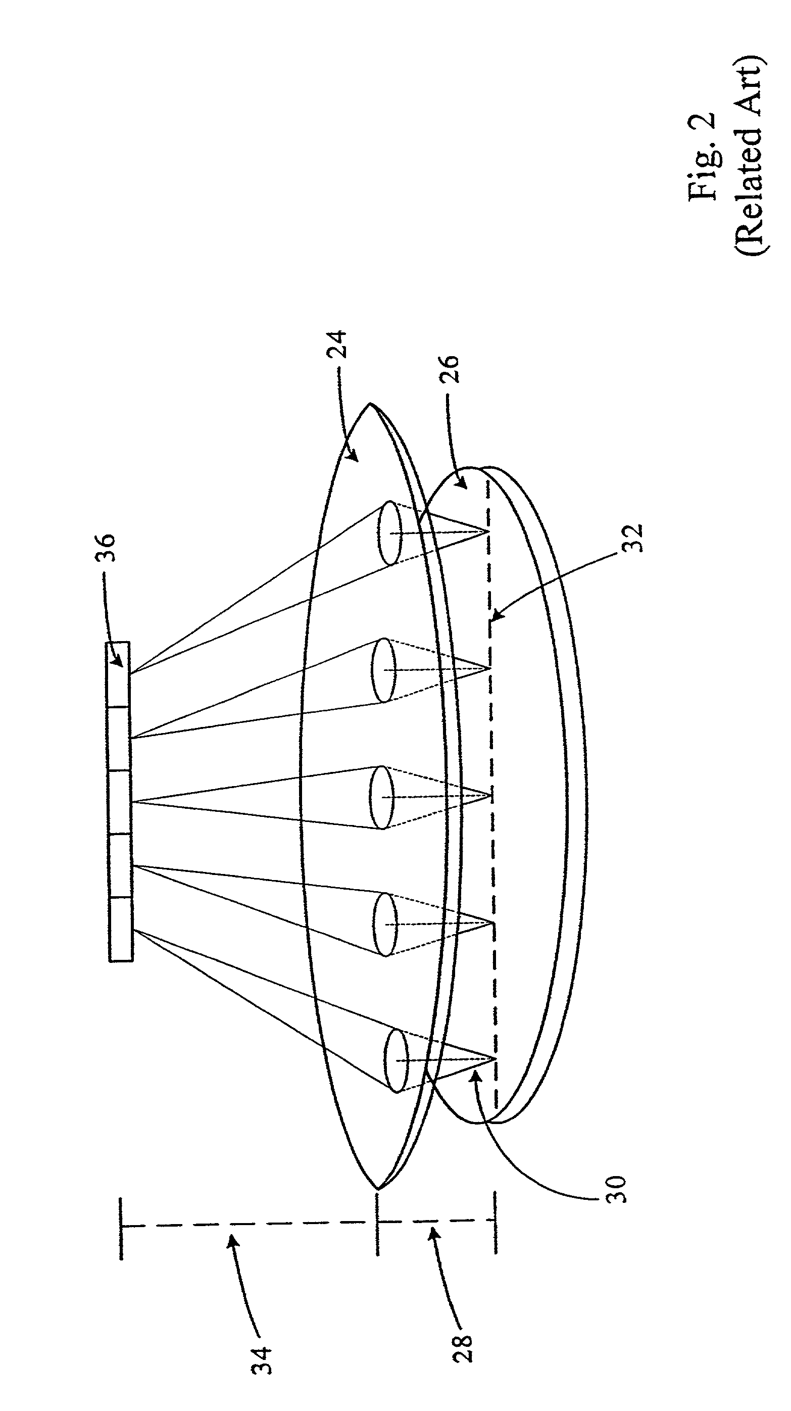
Such large
diameter optical components may be very expensive because the lenses need to be as large as the specimen.
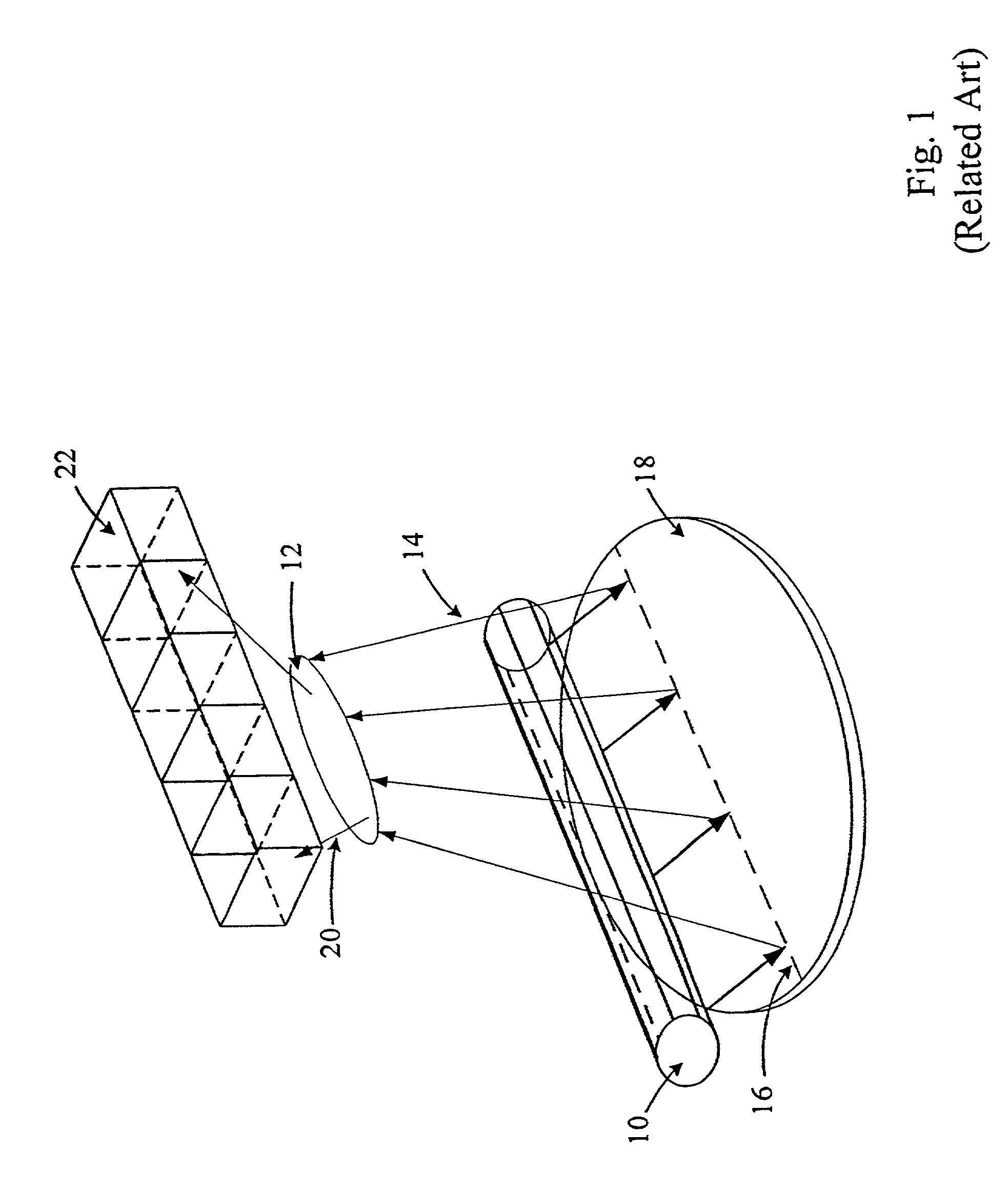
Large optical components such as mirror 38 and diffuser 48, however, can be very expensive.
Note that because conventional inspection systems typically have optical assemblies in which the illumination system and the detection system are separately mounted within the inspection system, often extensive calibration and
preventive maintenance work are required to ensure that the systems are performing adequately.
Inspection tools that have been developed for inspection of 200 mm semiconductor substrates may not be directly applicable in the semiconductor fabrication lines using 300 mm wafers, and thus may need to be completely, or at least significantly, redesigned to accommodate the new size and fabrication methodologies being introduced using 300 mm wafers.
However, several significant difficulties may arise in scaling current technologies.
For example, maintaining low fabrication costs for imaging lenses that are larger and in proportion to the
increased diameter of substrates and that maintain minimum
distortion may be extremely difficult.
An additional difficulty is ensuring equivalent or improved illumination uniformities for larger
diameter substrates.
Because some tools were intended to operate as stand-alone tools, these may have vertical and lateral dimensions that make integration into a semiconductor fabrication process line impractical.
If, for example, the illumination source is very dim, then the amount of time required to collect sufficient light for an image that can discern the defects of interest may be very long.
In the case of scaling conventional illumination system
optics and conventional detection system
optics to accommodate larger specimen sizes such as 300 mm wafers, delivery of sufficient light to the specimen surface and delivery of sufficient light to the detection sensors may become increasingly difficult without increase in the output of the illumination source itself.
Specifically, illumination using the same illumination source power and scaled optics may result in reducing the illumination per area by at worst the square of the ratio of specimen size differences, and at best as the ratio of the specimen size differences, depending on the size and shape of the illumination area.
This may increase cost.
Increased costs and / or complexity may result.

