Liquid crystal display device, electroluminescent display device, method of driving the devices, and method of evaluating subpixel arrangement patterns

a technology of electroluminescent display and liquid crystal display, which is applied in the direction of static indicating devices, identification means, instruments, etc., can solve the problems of high manufacturing cost, insufficient speed of data driver circuit, and significant increase in power consumption, so as to reduce power consumption and reduce power consumption of peripheral driver circuits , good image quality

Inactive Publication Date: 2006-08-01
JAPAN DISPLAY CENT INC
View PDF15 Cites 82 Cited by
  • Summary
  • Abstract
  • Description
  • Claims
  • Application Information

AI Technical Summary

Benefits of technology

[0101](1) The provision of a digital-to-analog converter circuit is unnecessary, and gray scale display is possible directly based on digital video data. Accordingly, digital-to-analog converter circuits as necessary in the prior art are eliminated, and thereby power consumption is reduced.
[0102](2) The occupied area and the power consumption of the peripheral driver circuits are reduced, and gray scale display with good image quality is achieved.
[0103](3) The number of voltage controlling capacitor lines is smaller than that in a configuration in which each voltage controlling capacitor is individually connected to each voltage controlling capacitor line. Therefore, an improvement in aperture ratio and a simplification of device drive controlling are achieved. In addition, the horizontal scanning frequency is reduced, and power consumption is thereby reduced. It may be possible to individually provide a storage capacitor line for each subpixel to achieve inversion driving for every other row of subpixels, but when employing a capacitively coupled driving method as in the present invention, such a configuration causes inferior y characteristic linearity because of the pixel electrode potent

Problems solved by technology

This incurs high manufacturing cost and considerable increase in power consumption.
(1) In the second prior-art example, both the scan driver circuit and the data driver circuit are formed of polycrystalline silicon. For this reason, when the number of pixels increases, that is, when the horizontal scanning time shortens as the number of pixels increases, the data driver circuit does not operate at a sufficient speed because the characteristics of polycrystalline silicon are inferior to those of single crystalline silicon.
(2) In the second prior-art example, in the case where each unit pixel is divided into a plurality of subpixels, the wiring configuration of data lines and scanning lines is such that the data lines are individually wired and the scanning lines are commonly wired. This structure significantly increases the number of connecting pins in the driver circuits, especially when each unit pixel needs to be further divided for R (red), G

Method used


Image

  • Liquid crystal display device, electroluminescent display device, method of driving the devices, and method of evaluating subpixel arrangement patterns
  • Liquid crystal display device, electroluminescent display device, method of driving the devices, and method of evaluating subpixel arrangement patterns
  • Liquid crystal display device, electroluminescent display device, method of driving the devices, and method of evaluating subpixel arrangement patterns

Examples


embodiment 1

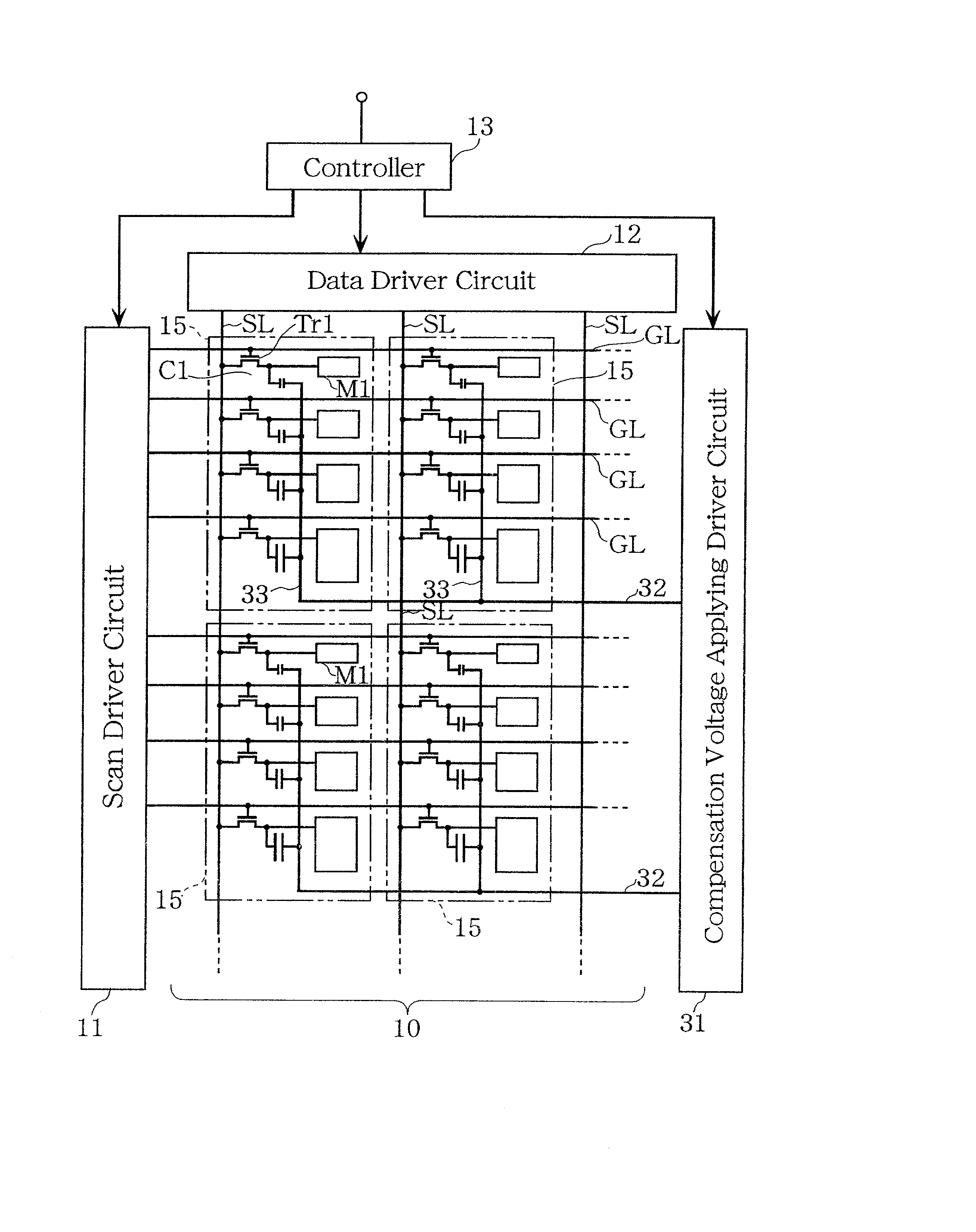
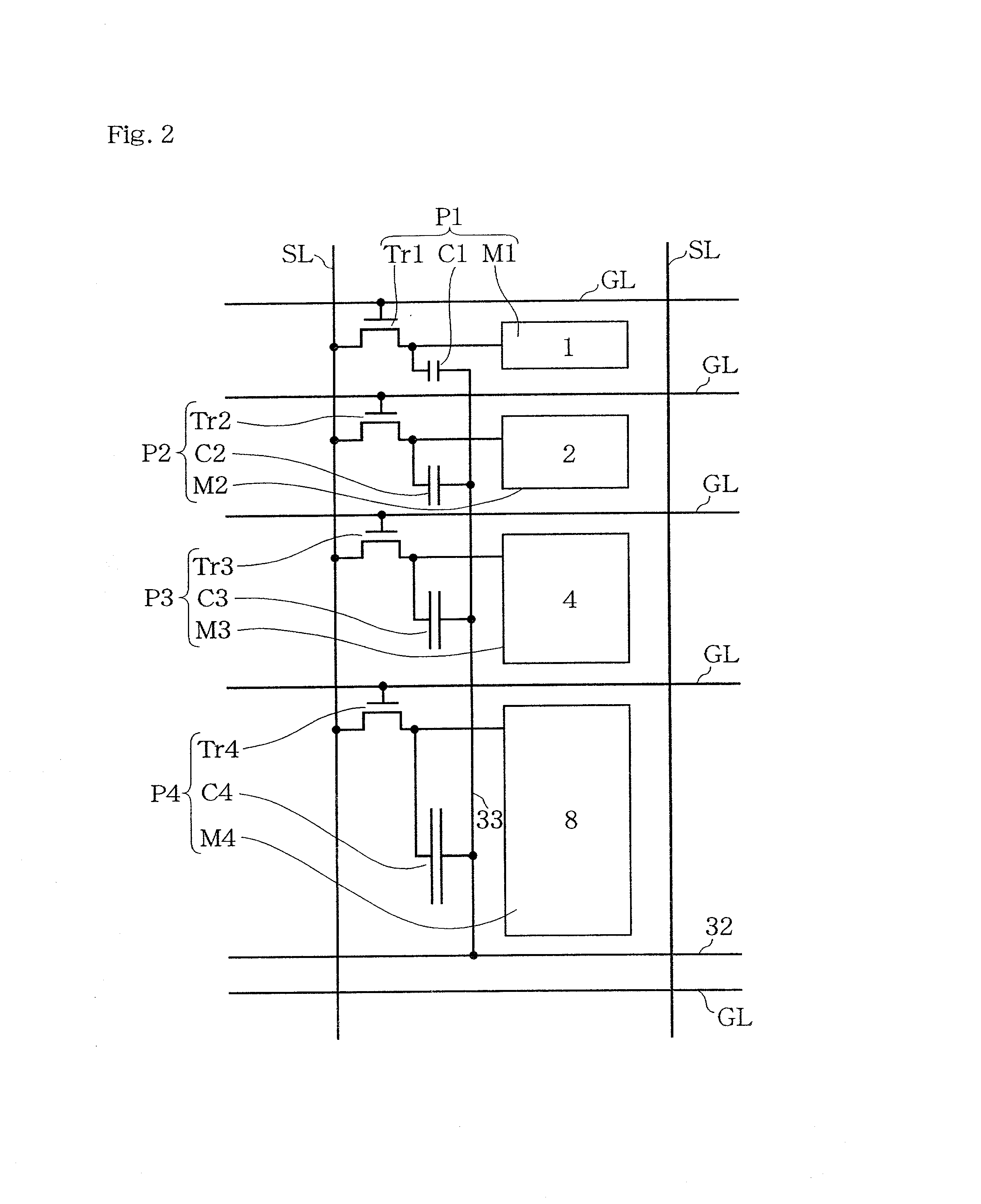
[0148]FIG. 1 shows a circuit diagram of a liquid crystal display device according to Embodiment 1 of the present invention. FIG. 2 shows a circuit diagram illustrating the configuration of a unit pixel. This liquid crystal display device is of a digital driving system type by which gray scale display is performed using a digital image signal. The digital image signal have 4-bit data format. The device is of an active matrix type and is capable of displaying 16 gray levels. Referring now to FIGS. 1 and 2, an example of the specific configuration of the device is discussed below. FIG. 1 illustrates a liquid crystal display unit 10 comprising a plurality of unit pixels 15 arranged in a matrix configuration, a scan driver circuit 11, a data driver circuit 12, a controller 13, and a compensation voltage-applying driver circuit 31 for supplying a compensation voltage signal to voltage controlling capacitor lines 32.

[0149]The liquid crystal display unit 10 has a plurality of source lines (...

embodiment 2

[0173]Embodiment 2 is characterized in that, in a liquid crystal display device according to the foregoing Embodiment 1, the capacitance values of the voltage controlling capacitors are optimized, and the voltage amplitude of the scanning signal is minimized within the range in which the liquid crystal can be driven, in order to achieve a further reduction in power consumption. The details are given below.

(1) Optimization of Voltage Controlling Capacitance

[0174]In a liquid crystal display device according to Embodiment 2, the voltage controlling capacitance Cc is determined by the following Equation (1):

Cc={(Vbias / Vepp−Vbias)}·(Clc+Cgd)  (1)

[0175]In Equation (1) above, Vepp denotes the amplitude of the compensation voltage, Vbias denotes the amount of variation of the pixel voltage caused by the variation of the compensation voltage, and Clc denotes the liquid crystal capacitance in each subpixel, and Cgd denotes the parasitic capacitance of the transistor.

[0176]The introduction of ...

embodiments 1 and 2

Supplementary Remarks for Embodiments 1 and 2

[0187]The liquid crystal display devices according to the above Embodiments 1 and 2 may be suitably applied to both transmissive and reflective type liquid crystal display devices. In particular, in cases of reflective type liquid crystal display devices, it is possible to provide large subpixel regions by disposing source lines SL, gate lines GL, pixel transistors Tr1 to Tr4, and voltage controlling capacitors C under the reflective pixel electrodes.

[0188](2) In the above-described embodiments, the scan driver circuit 11 is formed of polycrystalline silicon and the data driver circuit 12 is formed of single crystal silicon, but the present invention is not limited thereto. Both the scan driver circuit 11 and the data driver circuit 12 may be formed of polycrystalline silicon.

[0189](3) The liquid crystal display devices according to the present invention may be suitably applied to display devices for information terminal devices such as m...


PUM


Abstract

An active matrix liquid crystal display device has a plurality of unit pixels being arranged in a matrix configuration, each unit pixel being divided into a plurality of subpixels. Each of the subpixels has a subpixel electrode, a pixel transistor connected to the subpixel electrode, and a voltage controlling capacitor connected to the subpixel electrode. A voltage controlling capacitor line for supplying a compensation voltage signal is connected to the voltage controlling capacitor so that after the writing to the subpixel has been completed, the potential of the compensation voltage signal is varied to modulate the potential of the subpixel electrode to be a predetermined voltage, using the voltage controlling capacitor. Such combining of spatial dithering attained by a pixel-dividing technique and a capacitively-coupled driving method eliminates the need for digital-to-analog converter circuits, attains gray scale display based on a digital image signal, and achieves a reduction in power consumption.

Description

BACKGROUND OF THE INVENTION[0001](1) Field of the Invention[0002]The present invention relates to a liquid crystal display device and an electroluminescent (EL) display device, which are applicable to so-called mobile information devices or the like. The invention also relates to methods of driving the display devices. More particularly, the invention relates to a liquid crystal display device and an EL display device in which halftone display is performed by a spatial dithering method, and to methods of driving the devices and of evaluating subpixel arrangement patterns.[0003](2) Description of the Prior Art[0004]A conventional pixel circuit configuration for an active matrix liquid crystal display panel is shown in FIG. 39 (hereafter, the example of active matrix liquid crystal display panel depicted in FIG. 39 is referred to as “the first prior-art example”). FIG. 39 shows source lines (data lines) SL, gate lines (scanning lines) GL, a pixel transistor Tr, a storage capacitor C, ...

Claims


Application Information

Patent Timeline
IPC IPC(8): G09G3/36G02F1/1333G02F1/1362G02F1/133G02F1/1368G09F9/00G09F9/30G09F9/35G09G3/20G09G3/30G09G3/32H01L27/32H01L51/50H05B44/00
CPCG09G3/32G09G3/3655G09G3/3659G02F2001/134345G09G2330/021G09G3/2059G09G3/2074G09G3/3614G09G2300/0443G09G2300/0456G09G2300/0876G09G2310/0224G09G2320/0219G09G2330/02G09G3/2051G02F1/134345G09G3/20
Inventor SENDA, KOUJINANNO, YUTAKATAKEHASHI, SHIN-ITSU
Owner JAPAN DISPLAY CENT INC
Why Eureka
Try Eureka