Semiconductor device and method of manufacturing the same

a semiconductor and semiconductor technology, applied in the direction of transistors, optics, instruments, etc., can solve the problems of not being able to grow crystals with a particular orientation, not being able to control the producing position and density of crystal cores, and not being able to orient all surfaces of substrates, etc., to achieve the effect of improving the mobility of field effect and reducing the dispersion of characteristics between elements

Inactive Publication Date: 2006-09-19
SEMICON ENERGY LAB CO LTD
View PDF54 Cites 19 Cited by
  • Summary
  • Abstract
  • Description
  • Claims
  • Application Information

AI Technical Summary

Benefits of technology

[0013]As described above, in a conventional method of crystallization using a laser beam, variance (or dispersion) in a TFT characteristic becomes large, which causes various functions of a semiconductor device comprising TFTs as components of its electronic circuit to be restrained.
[0014]In view of the above problems, an object of the invention is to improve crystallinity of a crystalline semiconductor film formed by crystallizing an amorphous semiconductor film so as to provide a TFT capable of operating at higher speed.
[0016]Concretely, a first shape of semiconductor region having on its one side a plurality of sharp convex top-end portions (projections) is formed first and a continuous wave laser beam is used for radiation from the above region so as to crystallize or improve crystallinity of the first shape of semiconductor region along a scanning direction of the laser beam. Preferably, a continuous wave laser beam condensed in one or plural lines on a radiation surface is used for the laser beam. Then, the first shape of semiconductor region is etched to form on its inner side a second shape of semiconductor region on which a channel forming region and a source and drain region are formed. The second shape of semiconductor region has a plurality of oblong semiconductor regions so that a channel forming range would be formed on respective crystal regions extending from the plurality of convex end portions, and is etching-processed by means of a photoetching method so that a semiconductor region adjacent to the channel forming region would be eliminated. That is to say, a first shape of semiconductor region in which a plurality of semiconductor regions having on its one side a sharp convex top-end portion is disposed in parallel is formed from a semiconductor film formed on an insulating surface, and a continuous wave laser beam is used for radiation from the above first shape of semiconductor region so as to crystallize or improve crystallinity of the first shape of semiconductor region along a scanning route of the laser beam.
[0023]That is, a region provided with a channel forming area for a TFT in a second shape of semiconductor region is provided so as to be formed with good crystals extending from a plurality of sharp convex top-end portions in one end portion of the first shape pf semiconductor region. Alternatively, the region provided with a channel forming area is partly etched to in order to prevent a grain boundary extended from the concave portion or a distortion-accumulated crystal from overlapping a channel forming region.
[0024]In accordance with such a structure, a plurality of rectangular semiconductor regions are provided in parallel to form a transistor, so that dispersion of a characteristic between elements can be made small. Further, using only good crystals can improve mobility of field effect.

Problems solved by technology

It has not been possible, however, to orient all surfaces of a substrate to a particular single crystal orientation.
In most conventional methods, however, it is not possible to control producing position and density of a crystal core, so that crystallization has been performed by means of a naturally produced crystal core.
Therefore, there is a problem that a crystal cannot be grown with a particular orientation.
Usually, a large number of defects are produced in a grain boundary.
Moreover, the crystal orientation is random due to dependence on a crystal core produced at any time, so that the crystalline semiconductor cannot be oriented in a line.
In a laser process using a pulse width oscillation laser oscillator device, crystal growth caused by a crystal core is dominant, and thereby, a grain size cannot be enlarged in practice.

Method used


Image

  • Semiconductor device and method of manufacturing the same
  • Semiconductor device and method of manufacturing the same
  • Semiconductor device and method of manufacturing the same

Examples


embodiment 1

[0081]In this embodiment, an amorphous silicon film formed on an insulating surface is etched into a predetermined pattern in a photoetching method to form a first shape of semiconductor region, which is then crystallized by means of a continuous wave laser beam.

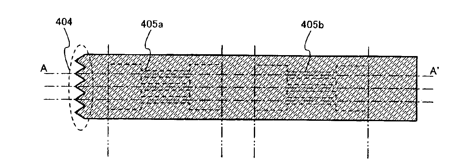
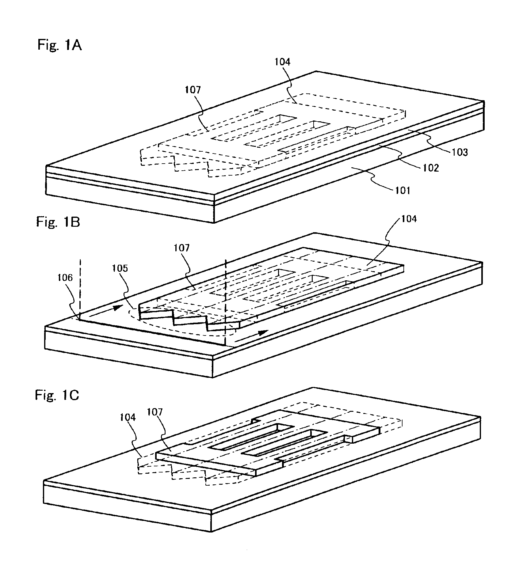
[0082]In FIGS. 8A and 8B, a barrier layer 402 consisting of a silicon oxide nitride film of 100 nm is formed on a glass substrate 401. A first shape of semiconductor region 403 on the barrier layer 402 is an amorphous silicon film formed by a plasma-CVD method into a thickness of 100 nm. FIG. 8A is a top view of the first shape of semiconductor region 403, while FIG. 8B shows a cross-sectional structure including a substrate. Second shape of semiconductor regions 405a and 405b for providing an active layer of a TFT are formed inside the first shape of semiconductor region 403 so as not to reach the end thereof, as shown by dotted lines, although they are not yet concretely expressed in this stage.

[0083]A region provided with...

embodiment 2

[0088]The scanning of the laser beam in the embodiment 1 may be scanned not only in one direction but also back-and-forth strokes. In this case, the seed regions 404a and 404b may be provided at both sides of the first semiconductor region 403 as shown in the embodiment of FIGS. 11A and 11B. In case of back-and-forth strokes, laser energy density is changed every stroke so that the crystal growth can be phased. The scanning of the laser beam also serves for hydrogen extraction treatment that is often required in case of crystallization of amorphous silicon film. After hydrogen is extracted by scanning at low energy density at first, the crystallization may be performed by the second scanning at higher energy density. This producing method also results in a crystal semiconductor film which crystal grains extend in the scanning direction of the laser beam.

embodiment 3

[0089]The embodiment 3 intends that an amorphous silicon film formed on an insulating surface is crystallized in advance and enlargement of a crystal grain by a continuous wave laser beam.

[0090]As shown in FIG. 12A, blocking layer 502 and a amorphous silicon film 503 are formed on a glass substrate 501 like the embodiment 1. A 100 nm thick oxide silicon film as a masking insulation film 504 is formed on the blocking layer 502 and the amorphous silicon film 503 by plasma CVD technique, and an opening 505 is provided. In order to add Ni as a catalytic element, water solution containing 5 ppm nickel acetate is spin-coated. Ni is in contact with the amorphous silicon film at the opening 505. A location where the opening 505 is formed is located in the seed region of the first semiconductor region that is formed later or out side of the seed region.

[0091]Then, as shown in FIG. 12B, the amorphous silicon film is crystallized by a 4 hours heat treatment at a temperature of 580° C. The crys...


PUM

PropertyMeasurementUnit
lengthaaaaaaaaaa
angleaaaaaaaaaa
absorption coefficientaaaaaaaaaa

Abstract

In a conventional method of crystallization using a laser beam, variance (or dispersion) in a TFT characteristic becomes large, which causes various functions of a semiconductor device comprising TFTs as components of its electronic circuit to be restrained.A first shape of semiconductor region having on its one side a plurality of sharp convex top-end portions is formed first and a continuous wave laser beam is used for radiation from the above region so as to crystallize the first shape of semiconductor region. A continuous wave laser beam condensed in one or plural lines is used for the laser beam. The first shape of semiconductor region is etched to form a second shape of semiconductor region in which a channel forming region and a source and drain region are formed. The second shape of semiconductor region is disposed so that a channel forming range would be formed on respective crystal regions extending from the plurality of convex end portions. A semiconductor region adjacent to the channel forming region is eliminated.

Description

BACKGROUND OF THE INVENTION[0001]1. Field of the Invention[0002]The present invention relates to a semiconductor device using a crystalline semiconductor film crystallized by radiating an amorphous semiconductor film with a laser beam and a method of manufacturing the same.[0003]2. Description of the Related Art[0004]There has been a known technology for crystallizing an amorphous semiconductor film formed on a substrate such as glass by means of a laser process. The laser process means a method of recrystallizing a damaged or amorphous film formed on a semiconductor substrate or a semiconductor film, a method of crystallizing an amorphous semiconductor film formed on an insulating surface or a method of improving crystallinity of a semiconductor film (crystalline semiconductor film) having a crystalline structure. A gas laser represented by an excimer laser or a solid laser represented by a YGA laser is usually used as a laser oscillator device used for the laser process.[0005]A fe...

Claims


Application Information

Patent Timeline
Patent Type & Authority Patents(United States)
IPC IPC(8): H01L21/00G02F1/1368H01L21/20H01L21/336H01L21/77H01L21/84H01L27/12H01L29/04H01L29/786
CPCH01L27/1214H01L27/1285H01L29/78675H01L29/66757H01L29/04H01L27/1222H01L27/127
Inventor KOKUBO, CHIHOSHIGA, AIKOYAMAZAKI, SHUNPEIMIYAIRI, HIDEKAZUDAIRIKI, KOJITANAKA, KOICHIRO
Owner SEMICON ENERGY LAB CO LTD
Why Eureka
Try Eureka