

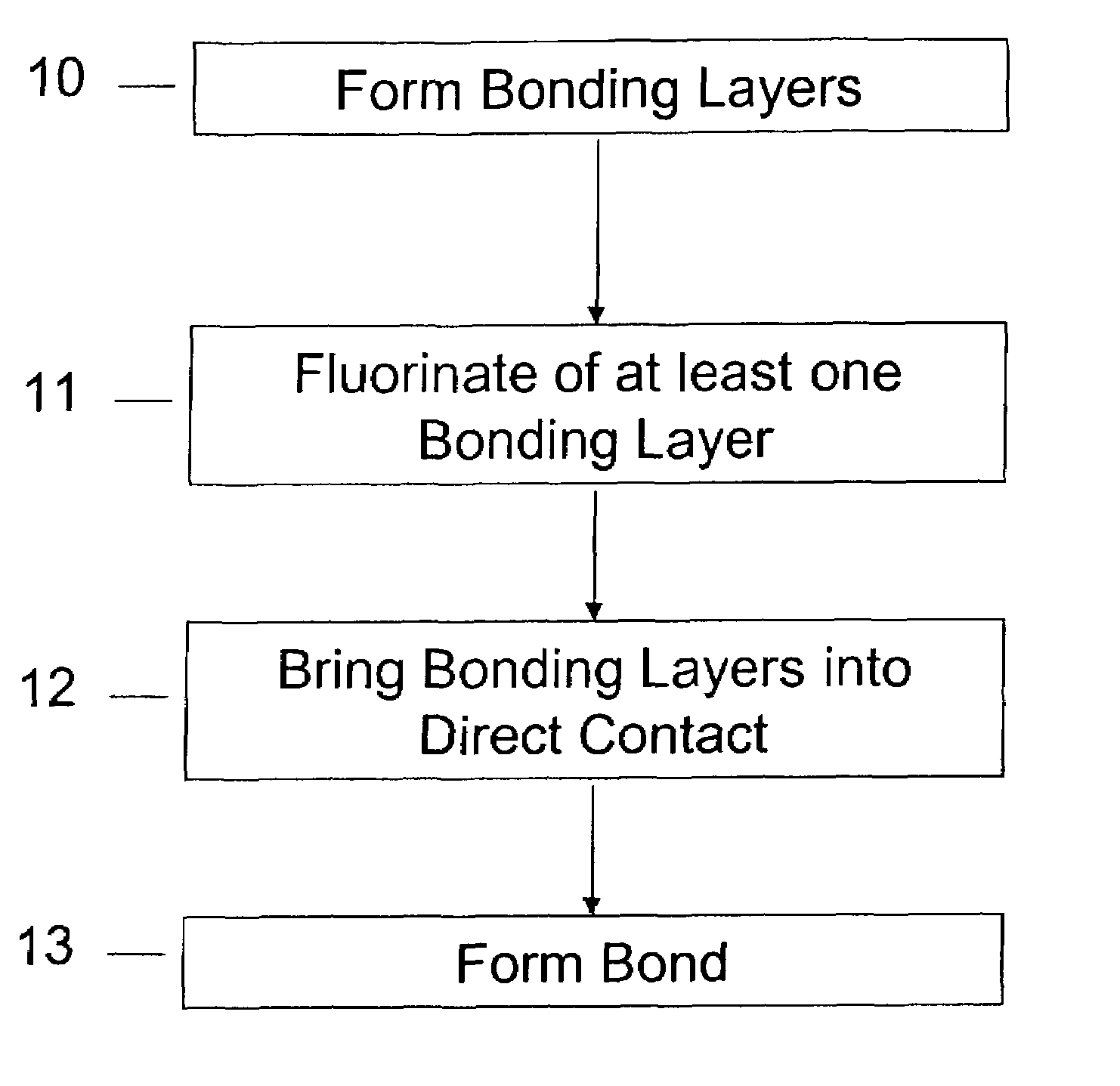
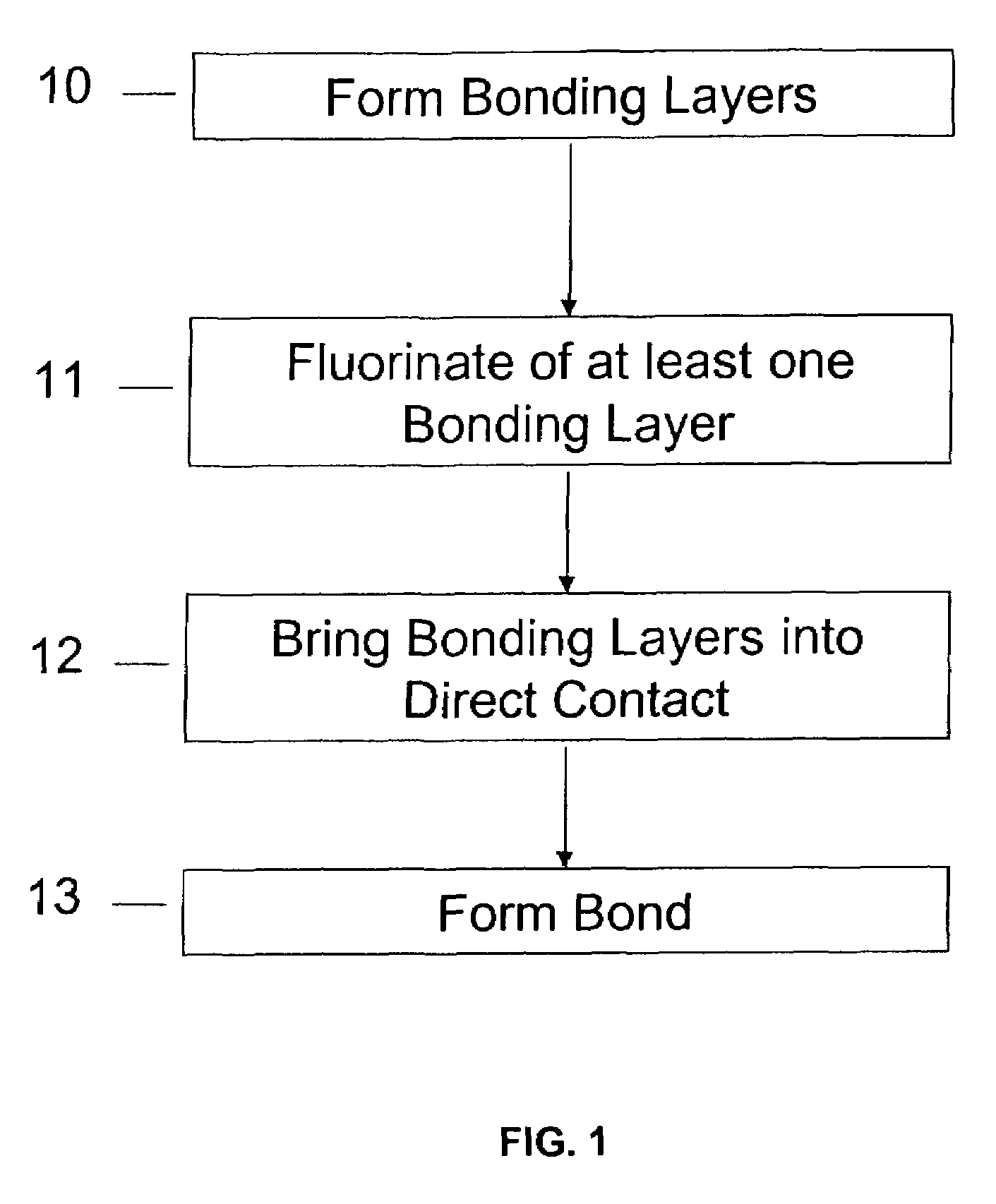
Method of room temperature covalent bonding
a covalent bonding and room temperature technology, applied in the direction of semiconductor/solid-state device details, transportation and packaging, coatings, etc., can solve the problems of high defect density of hetero-epitaxial grown films, difficult optimization, debonding or cracking, etc., to enhance the diffusion rate of impurities and/or moisture absorption, the effect of high covalent bonding density
- Summary
- Abstract
- Description
- Claims
- Application Information
AI Technical Summary
Benefits of technology
Problems solved by technology
Method used
Image

Examples
example
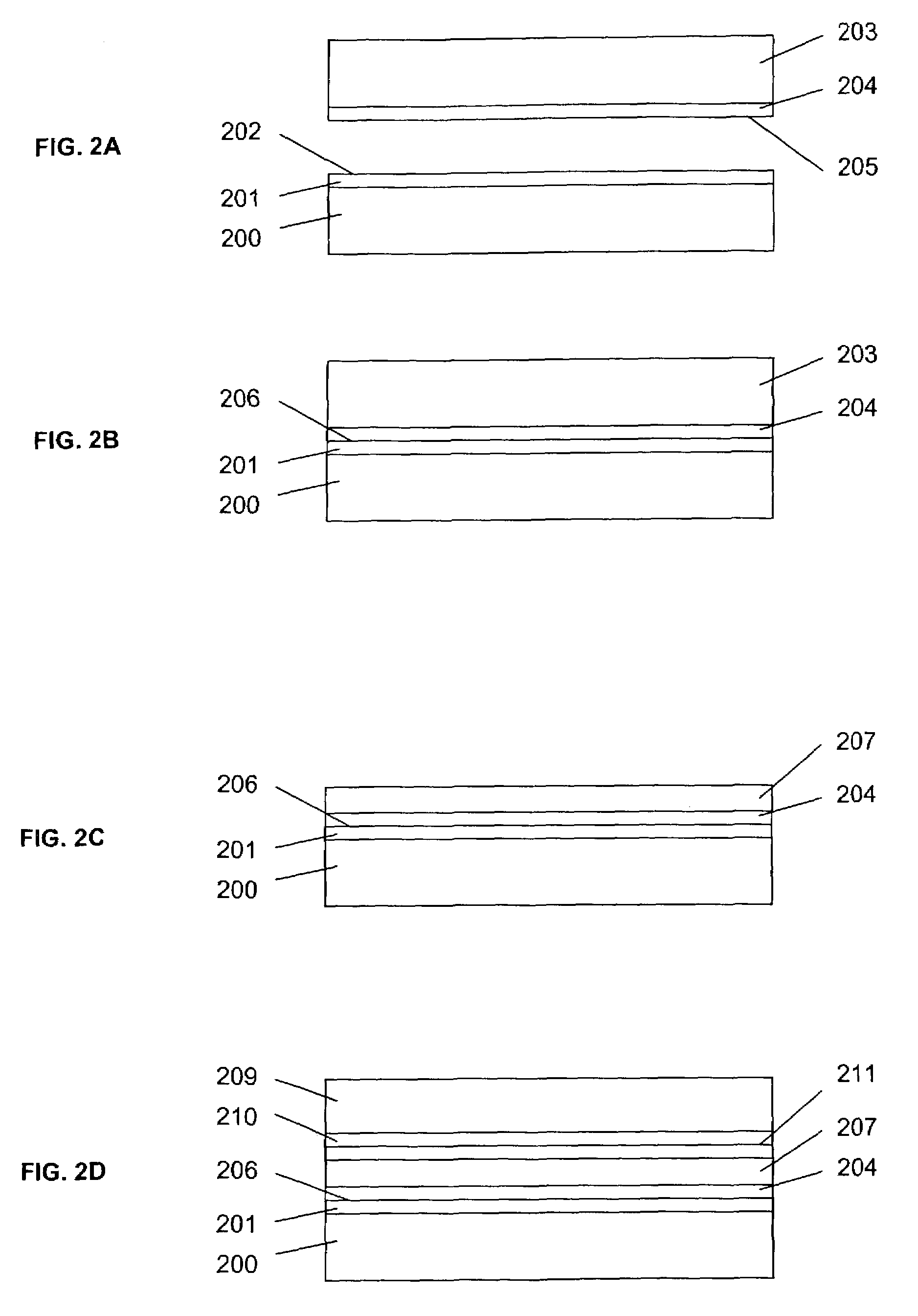
[0075]A second example of the method will be described again using FIGS. 8A–8C. A first oxide layer 81 is formed on substrate 80 (FIG. 8A). Fluorine is introduced into film 81 by one of the procedures described above, namely, exposure to HF or exposure to a F-containing gas. A second oxide film 82 is formed on film 81 by PECVD, for example (FIG. 8B). Fluorine is introduced into the second film by diffusion and / or surface segregation. It may also be introduced into the second film by the use of an appropriate F-containing precursor for the deposition of said oxide film 82. It is noted that the dimensions of films 81 and 82 are not to scale for this example, since the figures were also used to describe an example where film 82 is formed in the surface of film 81, but the figures do accurately represent the position of films 81 and 82. In this example, the structure does not need to be baked to create a fluorinated layer that assists in the removal of reaction byproducts because of the...
PUM
| Property | Measurement | Unit |
|---|---|---|
| surface roughness | aaaaa | aaaaa |
| temperature | aaaaa | aaaaa |
| temperature | aaaaa | aaaaa |
Abstract
Description
Claims
Application Information