Method for manufacturing optical bench, optical bench, optical module, silicon wafer substrate in which wiring and groove are formed, and wafer

a manufacturing method and technology for substrates, applied in the field of substrates, can solve the problems of difficult complete protection, extremely reduced coating performance, and difficult process difficulties, and achieve the effects of improving yield, shortening process time, and increasing process efficiency

Inactive Publication Date: 2006-10-10
MAXELL HLDG LTD
View PDF4 Cites 0 Cited by
  • Summary
  • Abstract
  • Description
  • Claims
  • Application Information

AI Technical Summary

Benefits of technology

[0012]The present invention has been made to solve the foregoing technical problems, and an object of the invention is to drastically increase efficiency in the manufacturing processes of a substrate in which a groove and a wiring are formed, and to facilitate improvement of the yield and shorten the process time.
[0013]Another object of the invention is to improve wiring accuracy in manufacturing an optical bench.
[0015]If the plating process forms the wiring pattern by electroless plating, the plating process is preferable, for example, because a reaction speed can be set at a low level, and a highly uniform film with a small residual strain can be obtained. Accordingly, a dense film, which is different from a microporous film in a sputtered film or the like, can be obtained, whereby any film damage such as pitting corrosion does not occur. Thus, corrosion resistance, including alkali resistance, which a metal originally has, can be exhibited. If the plating process includes a plurality of plating processes, at least one of which executes electroless plating processing on the wiring pattern without any masks, it is advantageous, for example, because etching work is more easily carried out on subsequent layers, which can be deposited in the same pattern, than in a stacked film, and dimension accuracy can be increased.
[0017]If the groove manufacturing process further comprises: a protective film forming process which coats the wiring pattern formed by the plating process with a protective film; and a protective film removing process which removes the protective film after the groove manufacturing process, the process is preferable because stronger resistance to the wiring can be obtained when the groove is manufactured in the Si substrate by a strong alkali. Especially, if the protective film forming process forms a protective film made of a metal containing nickel, it is advantageous in terms of the strong alkali resistance. However, the object of the invention can be achieved even without forming such a protective film.

Problems solved by technology

However, when the optical bench is mounted with a component having a wiring such as a laser diode, it has difficulties with the process.
Since a protective film such as a resist or the like also has no sufficient resistance to the strong alkali, complete protection is difficult.
For this resason, coating performance is extremely reduced, and alignment accuracy is lowered, thereby causing a reduction in yield and a reduction in wiring accuracy.
This film formation requires, for example, a high-temperature heat treatment of about 1100° C., thereby causing a reduction in process efficiency.
Additionally, the formation of the oxide film is all carried out in the thin film process of sputtering or the like, and not always satisfactory in terms of mass production efficiency.

Method used


Image

  • Method for manufacturing optical bench, optical bench, optical module, silicon wafer substrate in which wiring and groove are formed, and wafer
  • Method for manufacturing optical bench, optical bench, optical module, silicon wafer substrate in which wiring and groove are formed, and wafer
  • Method for manufacturing optical bench, optical bench, optical module, silicon wafer substrate in which wiring and groove are formed, and wafer

Examples


Embodiment Construction

[0032]Hereinafter, the present invention will be described in detail according to an embodiment shown in the accompanying drawings.

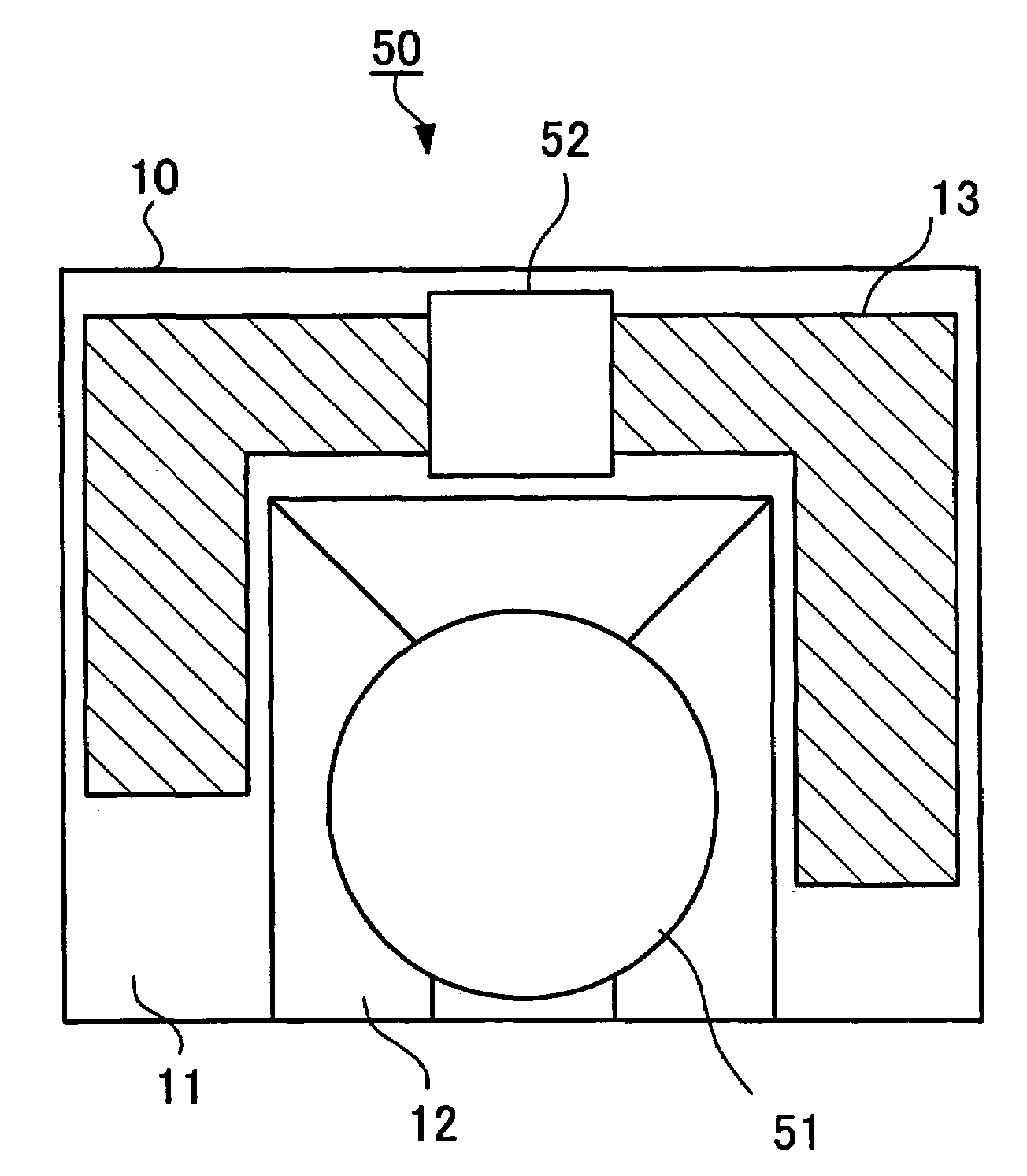
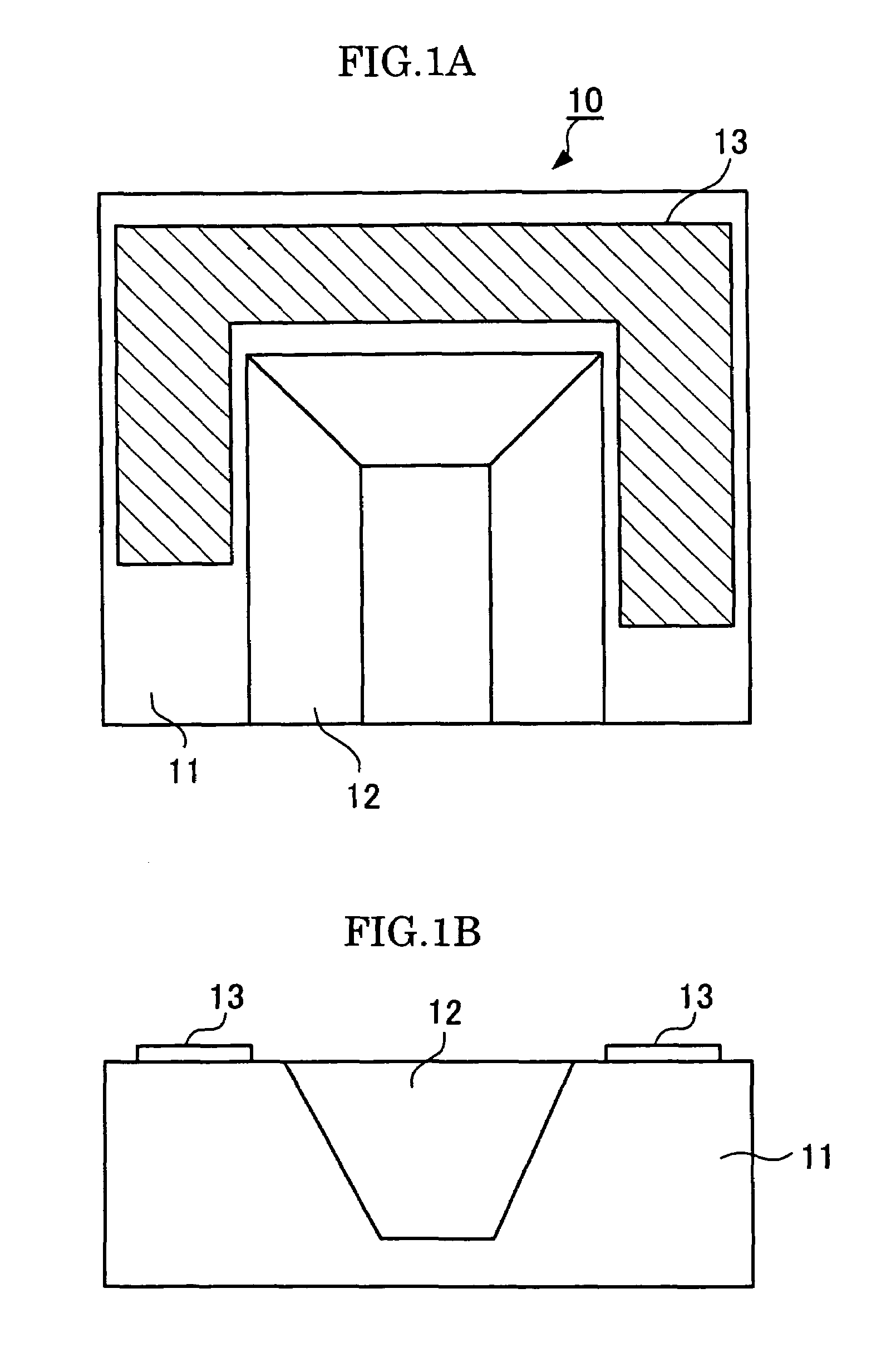
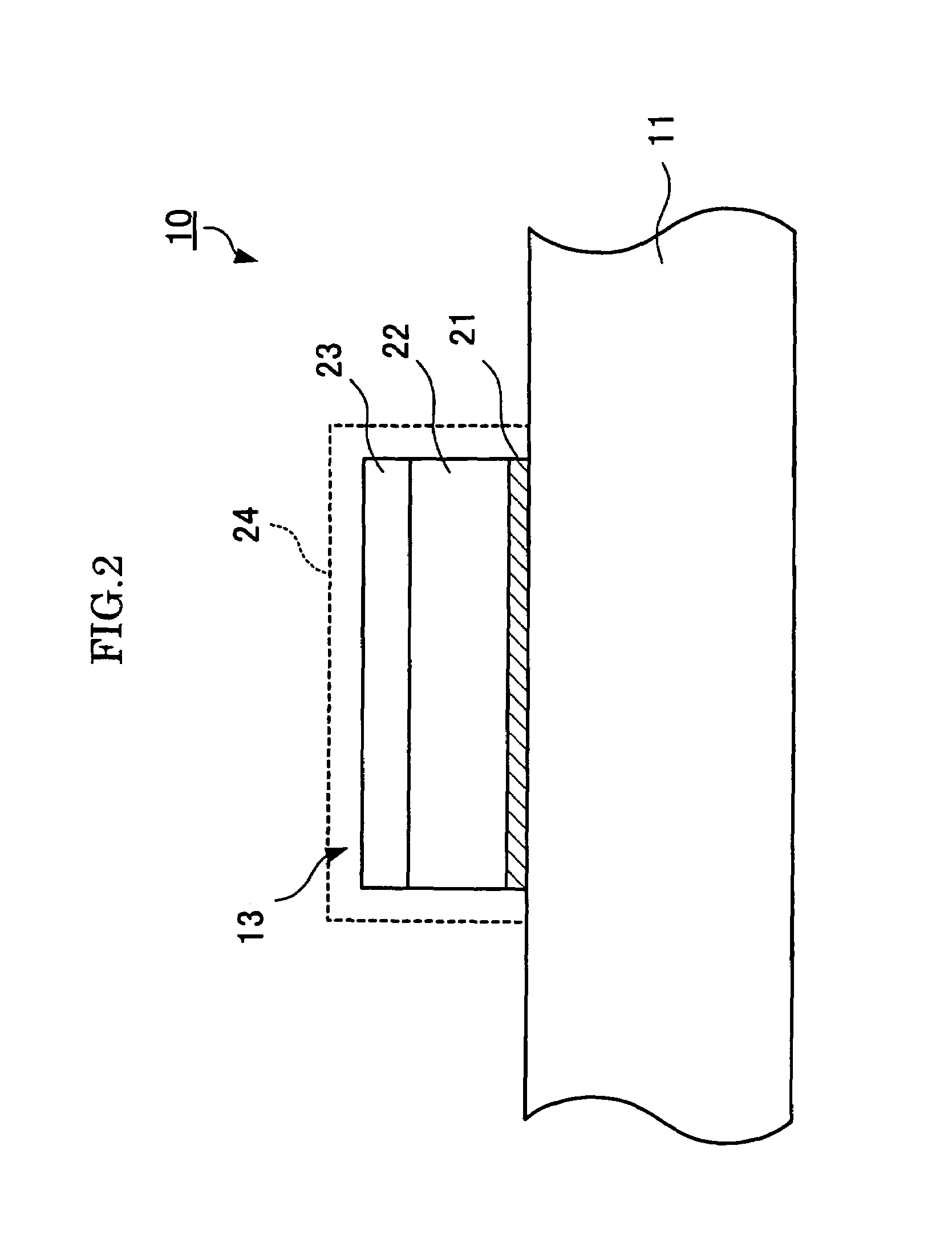
[0033]FIGS. 1A and 1B are views showing a constitution of an optical bench according to the embodiment. FIG. 1A is a top view of the optical bench, and FIG. 1B is a side view thereof. In an optical bench (silicon optical bench) 10 according to the embodiment, a groove 12, which is a deep groove for mounting an optical component such as a lens in position, is formed in an Si substrate 11, which is a silicon wafer. A wiring 13 is formed in a predetermined shape on the Si substrate 11. The embodiment has a feature that the wiring 13 is formed of plating. Further, according to the embodiment, in manufacturing processes to be described later, the groove 12 is formed after the formation of the wiring 13 on the Si substrate 11. As a result, the embodiment has another feature that no re-oxidation processing is executed after the formation of the groove 12, and n...


PUM

PropertyMeasurementUnit
temperatureaaaaaaaaaa
thicknessaaaaaaaaaa
thicknessaaaaaaaaaa

Abstract

An optical bench on which an optical component is mounted comprises an Si substrate made of a silicon wafer, a groove disposed on the Si substrate and designed to mount the optical component thereon, and a metal thin-film wiring for driving the optical component or a driver component. The metal thin-film wiring is formed in an electroless plating process before a groove manufacturing process which forms the groove by micromachining by means of wet processing.

Description

BACKGROUND OF THE INVENTION[0001]This Nonprovisional application claims priority under 35 U.S.C. § 119(a) on Patent Application No(s). 2003-165986 filed in JAPAN on Jun. 11, 2003, the entire contents of which are hereby incorporated by reference.[0002]The present invention relates to a substrate to mount, e.g., an optical component thereon, and a manufacturing method thereof or the like. More particularly, the invention relates to a substrate in which a wiring is formed and a predetermined groove is manufactured, and a manufacturing method thereof or the like.[0003]A recent progress in the optical communication technology has increased needs for, e.g., various components and devices used for a network, and optical modules using the same, and research and development have been actively conducted. Especially, a module, in which components such as an optical fiber, a lens, and a laser diode are appropriately combined, has been often used as a basic component.[0004]As a conventional tec...

Claims


Application Information

Patent Timeline
Patent Type & Authority Patents(United States)
IPC IPC(8): H01L21/00H01L21/311H01L21/76B81C1/00G02B6/36
CPCB81C1/00539B81B2201/047G02B6/3652G02B6/3692
Inventor FUKAO, RYUZOUSANBE, TETSUHIKO
Owner MAXELL HLDG LTD
Why Eureka
Try Eureka