Wafer processing method

a processing method and wafer technology, applied in the field of wafer stage structures, can solve the problems of increased complexity of work required therefor, deterioration of the wafer, and limitation of usable materials in the connection due to welding, so as to improve the uniformity of the wafer temperature, and improve the in-plane temperature distribution of the wafer

Inactive Publication Date: 2006-11-21
HITACHI HIGH-TECH CORP
View PDF10 Cites 53 Cited by
  • Summary
  • Abstract
  • Description
  • Claims
  • Application Information

AI Technical Summary

Benefits of technology

[0010]Additionally with this example, a method for improving a wafer in-plane temperature distribution is shown, wherein, for the purpose of improving the uniformity of a wafer temperature in the area of a wafer surface, a region with a variable height is provided within the region of a recess portion as provided in a cooling member causing thermal conductance between the cooling member and support member to have a distribution, thereby to improve the wafer in-plane temperature distribution. However, with such an arrangement, in the event that a cooling member structure capable of realizing an optimized temperature distribution is employed in the case of a certain use temperature, the wafer in-plane temperature distribution can often vary at other use temperatures. This phenomenon poses a serious problem in particular in the case of usage at a high temperature of 400° C. or 500° C. This can be said because heat release or “escape” of via radiation from the wafer stage relatively increases in the temperature region of 400° C. or 500° C. and thus serves as the cause of deterioration of the wafer in-plan temperature distribution. Inherently it is desirable that the temperature distribution of the wafer stage be kept uniform in a wide temperature range. To this end, it is advantageous that such heat release from the wafer stage is less whereas heat delivery between it and the cooling member stays uniform in the plane. However, in this example, no teachings are found as to methodology for suppressing the heat release from the wafer stage. The present invention was made in view of these problems to provide a wafer stage capable of uniformly maintaining the temperature distribution of a wafer at high temperatures within a wide temperature range. The invention also provides a wafer processing method with virtually no risks of giving obstruction to the wafer due to a temperature change during wafer processing using the wafer stage.

Problems solved by technology

In case the pedestal and heat sink are fixed together by welding techniques, whenever the wafer-supporting pedestal is replaced with a new one due to its lifetime or accidental failures or the like, a replacement range tends to become wider resulting in an increase in complexity of works required therefor.
Additionally the connection due to welding suffers from a limitation to usable materials—that is, both the pedestal and the heat sink are strictly required to be made of metals only.
This phenomenon poses a serious problem in particular in the case of usage at a high temperature of 400° C. or 500° C. This can be said because heat release or “escape” of via radiation from the wafer stage relatively increases in the temperature region of 400° C. or 500° C. and thus serves as the cause of deterioration of the wafer in-plan temperature distribution.
However, in this example, no teachings are found as to methodology for suppressing the heat release from the wafer stage.

Method used


Image

  • Wafer processing method
  • Wafer processing method
  • Wafer processing method

Examples


first embodiment

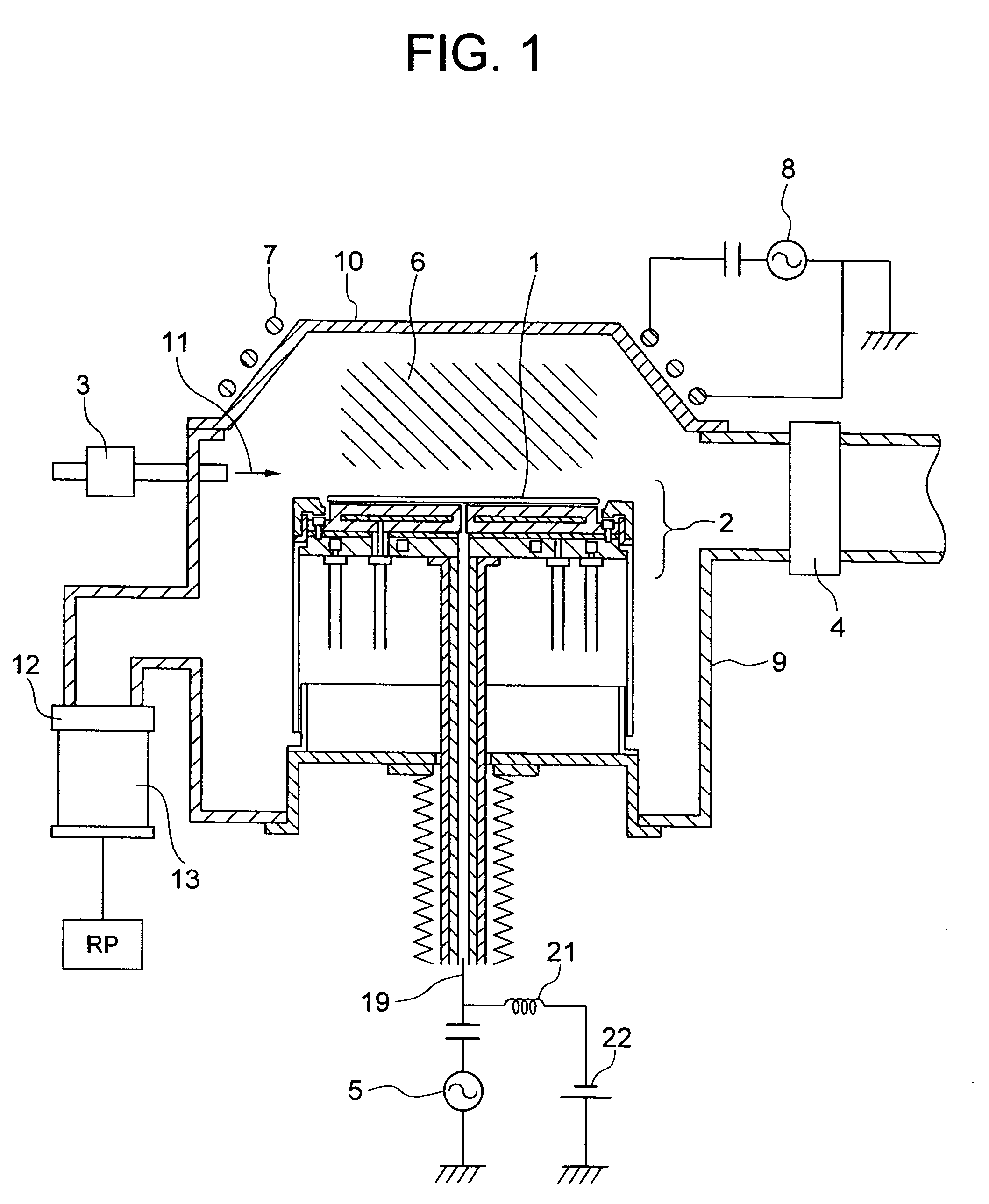
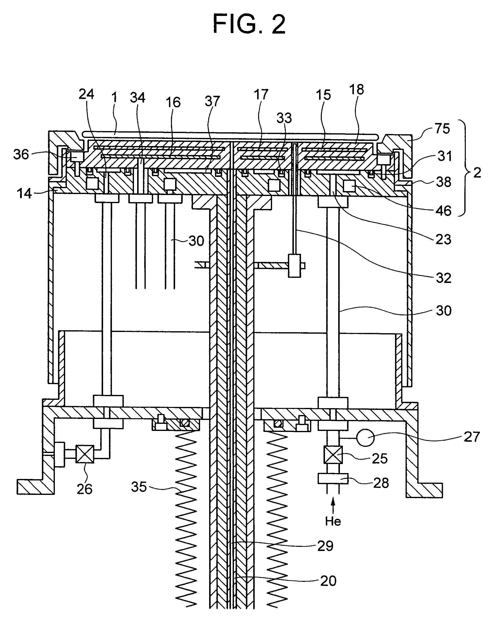
[0031]Preferred embodiments of the present invention will be explained with reference to the accompanying drawings below. this invention is shown in FIGS. 1 and 2. FIG. 1 depicts an example wherein a wafer stage of the invention is applied to a plasma processing apparatus; FIG. 2 shows an enlarged view of the wafer stage shown in FIG. 1; and, FIG. 3 is a perspective view of a water-cooling jacket.

[0032]As shown in FIG. 1, an etching gas 11 is introduced into the interior space of a vacuum chamber 9 while maintaining the chamber interior at an appropriate pressure by open-degree adjustment of a valve 12 that is installed in the upstream of a turbo molecular pump 13. A bell jar 10 made of alumina is stacked at upper part of the vacuum chamber 9, with a coil 7 mounted around this bell jar. The coil 7 is connected to a high-frequency power supply 8 for application of a high-frequency voltage, e.g. high-frequency voltage of 13.56 MHz, to both ends of the coil to thereby create an inducti...

second embodiment

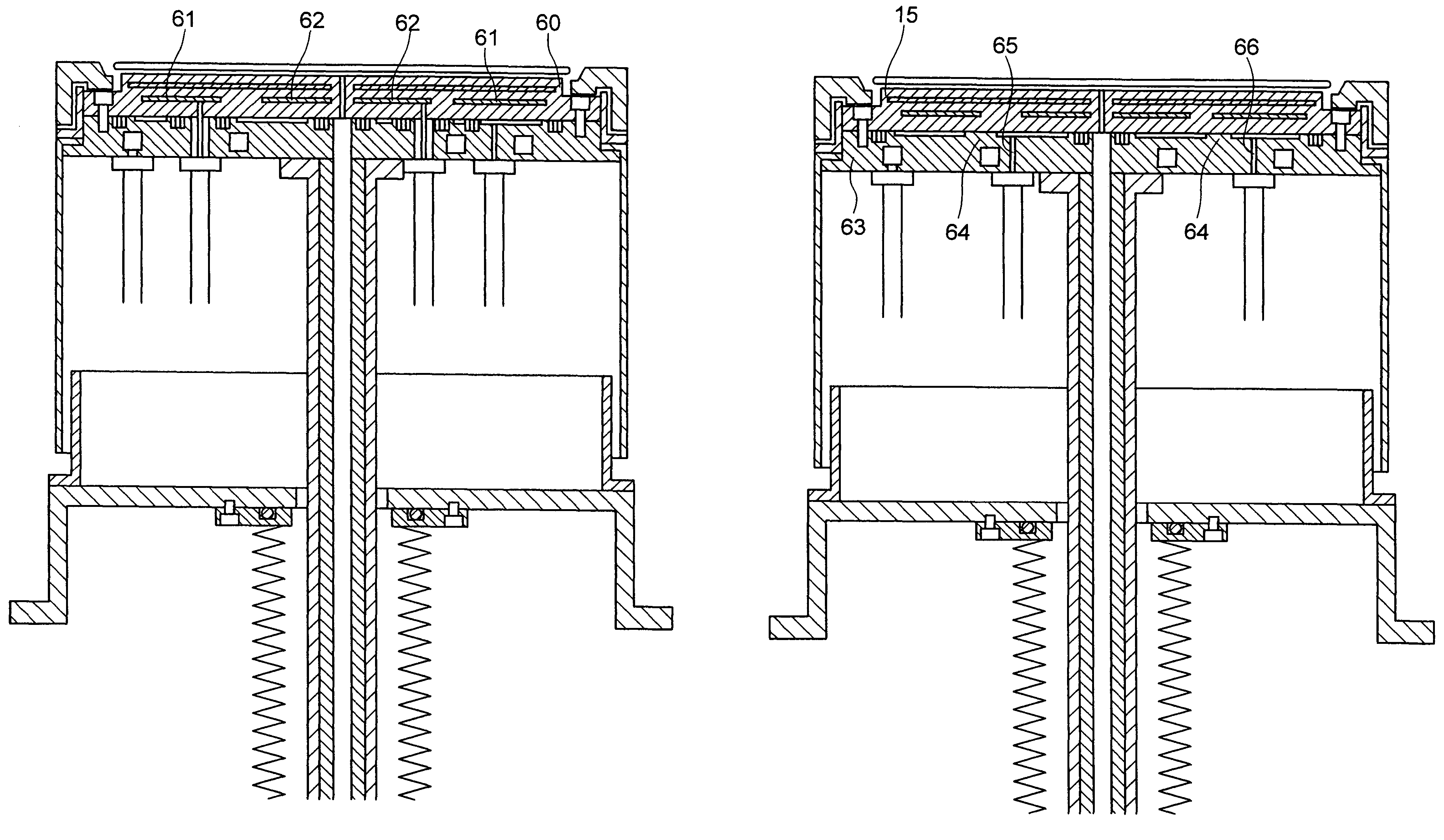
[0070]FIG. 12 shows the invention as disclosed and claimed herein. This embodiment is arranged to have a structure in which a heater assembly being internally provided in a ceramics plate 60 consists essentially of separate or “independent” heaters: an outer periphery heater 61, and an inner periphery heater 62. In addition, although not specifically depicted in FIG. 12, two sheath thermocouples are provided at locations in a radial direction for measurement of a temperature adjacent to the inner periphery of a wafer and a temperature near the outer periphery thereof. Using these two thermometers makes it possible to control electrical power being supplied to each heater on the basis of information as to temperatures as measured thereby. Note that in FIG. 12, a pusher pin mechanism is eliminated from the illustration for simplification purposes only.

[0071]With such an arrangement, in the event that a temperature distribution is required to be generated within a wafer surface, it bec...

third embodiment

[0073]the invention is shown in FIG. 13. In this embodiment a recess portion 64 is provided in the gap as provided between a water cooling jacket 63 and ceramics plate 15 in such a way as to permit division of an inner periphery and outer periphery while providing a mechanism for introduction and outward delivery of helium independently of the inner periphery and outer periphery. In the drawing, only an inside introduction port 65 and outside introduction port 66 are depicted with no helium exit ports shown therein. Note that the pusher pin mechanism and heater power feed unit are eliminated from the illustration for purposes of simplification only. In this arrangement, letting the inside region and outside region change in helium gas pressure makes it possible to permit thermal conductance relative to the ceramics plate to change accordingly, which in turn enables successful control of the resultant wafer temperature distribution. Although in this embodiment no specific seals are p...


PUM

PropertyMeasurementUnit
temperaturesaaaaaaaaaa
temperatureaaaaaaaaaa

Abstract

A wafer processing method for use with a wafer processing apparatus having a liquid cooling jacket with a built-in coolant liquid circulation path and a ceramic plate as attached onto the liquid cooling jacket and having therein a heater and an electrode for an electrostatic chuck. The method enables performance of wafer processing while letting a wafer be mounted on the ceramic plate by a wafer transport. The method includes causing the wafer transport to transport the wafer onto the ceramic plate, pre-heating the wafer while the wafer is held on the ceramic plate for a predetermined length of time, and mounting the preheated wafer on the ceramic plate.

Description

CROSS REFERENCE TO RELATED APPLICATION[0001]This is a continuation of U.S. application Ser. No. 10 / 087,747, filed Mar. 5, 2002, now U.S. Pat. No. 6,646,233, the subject matter of which is incorporated by reference herein.FIELD OF THE INVENTION[0002]The present invention relates generally to wafer stage structures for use in wafer processing apparatus, and more particularly to a wafer stage suitable for processing at high temperatures (ranging from about 200 to 500° C.).BACKGROUND OF THE INVENTION[0003]In recent years, certain materials including but not limited to ruthenium and its oxides or platinum or the like are thought to be the top-rated candidates for the capacitor electrode material of semiconductor devices of the next generation, owing to congeniality with currently available capacitor dielectric films high in dielectric constant and the like. In addition, materials which are considered to be employable as gate dielectric films in place of silicon oxides may include zirconi...

Claims


Application Information

Patent Timeline
Patent Type & Authority Patents(United States)
IPC IPC(8): F27B5/14H01L21/00H01L21/683
CPCH01L21/67109H01L21/6831
Inventor KANNO, SEIICHIROYOSHIOKA, KENNISHIO, RYOJIKANAI, SABUROUKIHARA, HIDEKIOKUDA, KOJI
Owner HITACHI HIGH-TECH CORP
Why Eureka
Try Eureka